Download
1 / 37
370 likes | 569 Views
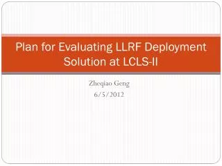
LCLS-II Injector LLRF System – MicroTCA Based Design. Zheqiao Geng 6/4/2012. LCLS-II Injector. The Injector Klystron Stations 10-6 for RF Gun 10-7 for L0A 10-8 for L0B 10-5 for TCAV0. Outline. Introduction Requirements Scope Architecture and Design Cost and Schedule

E N D
LCLS-II Injector LLRF System – MicroTCA Based Design ZheqiaoGeng 6/4/2012
LCLS-II Injector • The Injector Klystron Stations • 10-6 for RF Gun • 10-7 for L0A • 10-8 for L0B • 10-5 for TCAV0
Outline • Introduction • Requirements • Scope • Architecture and Design • Costand Schedule • Lessons Learnt from LCLS • Summary
Introduction • A quick comparison of PAD/PAC and MicroTCA solutions
Introduction (cont.) • Goals of the new MicroTCA design for LCLS-II Injector LLRF System compared to the design of LCLS LLRF and the LCLS-II LLRF baseline: • Improve RF stability by introducing intra-pulse feedback for both amplitude and phase control • Improve operability, upgradability, reliability, visibility, maintainability and availability • GUI will be redesigned to be more friendly to the users • More automation will be provided for LLRF operations • MicroTCA provides much overhead in computation power and data transfer speed which make the future upgrade of the system easier • Simplified system architecture (less chassis, less internal cabling) and built-in redundancy features of MicroTCA will improve the reliability of the system • IPMI of MicroTCA provides much more visibility and controllability of the system with platform diagnostics and board level remote control • Separation of analog parts which are installed in chassis with water cooling and digital parts which are installed in MicroTCA crate make maintenance easier • Hot-swap capability of MicroTCA reduces the mean time for repair and improves the availability of the system
Physics Requirements • LCLS-II requirements fall within LCLS 1 Requirements • LCLS-II CDR – Table 6.11 • Laser to Gun timing jitter: < 200fs rms • L0 Phase jitter: < 0.1degS rms • L0 amplitude error: < 0.07% rms • Requirements for LCLS-II Injector Transverse RF Deflector - PRD • TCAV0 Phase Jitter: < 500fs rms
Functional Requirements • The functional requirements to LCLS-II LLRF System are identical to LCLS LLRF System • Services: Provides RF frequencies to different systems; Acts as RF actuators for Fast Feedback System • Controls: Maintains phase and amplitude stabilities for Drive Laser Systems and HPRF stations; Sets phase and amplitude for them • Diagnostics: Measures RF phase and amplitude; Diagnoses status of Drive Laser Systems and HPRF stations; Diagnoses status and performance of itself
Scope • LLRF Frequency Reference providing various frequencies used at LLRF System, Timing System, Drive Laser Systems and others • Measurement and control of Driver Laser Systems • Measurement and control of HPRF (High Power Radio Frequency) stations of RF Gun, L0A, L0B and TCAV0 • Measurement of Beam Phase Cavity 1
Hardware Architecture and Design for LCLS-II Injector LLRF System
Architecture – LLRF Frequency Reference Improvements to LCLS Design • Redesign “476 MHz PLL” to replace the 119 MHz VCO with 476 MHz one to avoid phase uncertainties after power cycles • “LO and Clock Generator” provides both 119 MHz and 102 MHz clock to have more flexibilities in sampling rate • “LO and Clock Generator” and “Laser Ref Generator” use resettable frequency dividers to avoid phase uncertainties after power cycles • Measure 476 MHz signals for diagnostics • Add IPMI interface to all chassis
Design – LLRF Frequency Reference • LLRF Frequency Reference will follow the existing design of LCLS (also the baseline of LCLS-II LLRF), which consists of 14 Chassis located in the RF Hut • Low Risks – No recent failures in the proven system. • Low noise system – Integrated Noise from 10Hz to 10MHz is <30fs. 2856MHz : 22fSrms 10Hz to 10MHz 2830.5MHz : 22fSrms 10Hz to 10MHz
Design – SPAC • Use existing PAC design of LCLS (also the baseline of LCLS-II LLRF) – Build 4 Chassis • Low Risk - LCLS has had 0 PAC chassis failures since it began operations • SPACs are kept for LLRF Frequency Reference control to decouple it from the klystron controls which are done by the MicroTCA system. Reference control is relatively simple but should be more robust to keep the reference system continuously working. MicroTCA system tends to be maintained during MD days which may interrupt the RF operation. It is not acceptable for the LLRF Frequency Reference system.
Architecture – High Power RF Station Control • Similar architecture used for the control of Gun, L0A, L0B and TCAV0
Design – RF Support Chassis • Use existing RF Support Chassis design for LLRF AIP (new design compared to LCLS-II LLRF baseline) – Build 5 Chassis • 10 down mixers, 1 up converter and 1 klystron beam voltage conditioner • Low Risk –RF Support Chassis only combines the analog modules in LCLS PAD and PAC. No failures from beginning (Nov. 2011) of the test at LI28-2
Design – MicroTCA System • Extend existing MicroTCA design for LLRF AIP (new design compared to LCLS-II LLRF baseline) – Need 1 12-slot Crate • Risk – 6-slot systemhas been proved working at LI28-2. 12-slot system has been successfully demonstrated at DESY; EVR AMC/RTM boards still under development Vadatech MCH UTC002 ADLINK AMC-1000 CPU
Design – MicroTCA System (cont.) • AMC ADC Board (Struck SIS8300, Commercial) – Need 6 boards for injector LLRF • 4 lane PCI Express Connectivity • 10 Channels 125 MS/s 16-bit ADC • Two 16-bit DACs for Fast Feedback Implementation • Twin SFP Card Cage for High Speed System Interconnects • Virtex5 FPGA
Design – MicroTCA System (cont.) • AMC Timing Module (University of Stockholm) – Need 1 board for injector LLRF • Fiber optic links w/ drift compensation • ps stability • AMC module is receiver and transmitter • Clock, trigger and event distribution MTCA.4 (MicroTCA for Physics) version and RTM is under development at DESY
Design – Solid State Sub-booster • Use the same design of LCLS (also the baseline of LCLS-II LLRF) • 1kW amplifier to drive 5045 klystron • Four Injector S-Band Stations • Gun, L0A, L0B, and TCAV0 • This amplifier has no internal diagnostics • Input and out power is measured by the MicroTCA System • Low Risk - 9 of these units have been running since LCLS started operation without a failure • SLAC purchases module and installs in chassis with power supplies and sequencing relays
Architecture and Design of Firmware • General and configurable FPGA firmware for SIS8300 boards • Extend the FPGA firmware designed for LLRF AIP project • Work for all RF stations with proper configuration • Implement intra-pulse feedback for both amplitude and phase control • 64K data acquisition buffers for diagnostics • Arbitrary waveform generation from DACs
Architecture and Design of Software • Software is deployed to MicroTCA CPU and MCC Servers • Linux kernel drivers have been provided by hardware vendors • “AMC EVR Board Device Driver” and “BSA” LLA module will be provided by Timing System (out of LLRF scope) • “AMC ADC Board Device Driver” will use the existing implementation for LLRF AIP project • Existing LCLS PAC device driver will be used for “SPAC Device Driver” • “IPMI Device Driver” is under development • LLA of “Pulse-pulse RF Controller” will use the existing implementation for LLRF AIP project • A “System Manager” will be implemented for system status diagnostics and hardware/software management • “Automation”, “Algorithms and Procedures” and “GUI” will use the existing implementation for LLRF AIP project but need some development
GUI – Data Acquisition • Save all phase and amplitude values of the RF signals for the same RF pulse synchronously up to 65536 pulses • Save all waveforms for the same RF pulse synchronously up to 2048 pulses
LCLS-II Injector LLRF System Costs Comparison of overall cost of PAD/PAC solution and MicroTCA solution Assume the labor rate is $117/hour for Engineer and $81.8/hour for Technician.
LCLS-II Injector LLRF System Costs Hardware Cost for Special Parts of PAC/PAD and MicroTCA solutions
LCLS-II Injector LLRF System Costs (cont.) Labor Cost for Special Parts of PAC/PAD and MicroTCA solutions
LCLS-II Injector LLRF System Costs (cont.) Hardware Cost for Common Parts of PAC/PAD and MicroTCA solutions Labor Cost for Common Parts of PAC/PAD and MicroTCA solutions
Schedule • Upgrade/design of hardware, firmware and software will be done by Jan. 2013 • All hardware will be ready for rack installation by Oct. 2013 • Both hardware and software will be integrated and tested at lab by Feb. 2014 • Hardware and software will be installed in the RF HUT and ready for commissioning by Mar. 2014
Lessons Learnt from LCLS • The PAD/PAC based architecture is a bottleneck for real-time performance • ColdFire MCU is a major limitation of computation power, memory size and data transfer speed. PAD has limitations for 120 Hz waveform acquisition • Each PAD only has 4 ADC channels occupying 2U or 3U space in the rack. The ADC channel intensity is low which also makes reference tracking difficult because we can not have the reference signal measured by each PAD • A local feedback loop has to follow the path of PAD – VME – PAC with Ethernet connections. The system architecture is complex and the Ethernet communication is not robust • PAD and PAC chassis are hard to maintain after installed in the rack with cooling water connected • Software for PAD/PAC/VME system is complex. There are many pieces of software interconnected with UDP which are unnecessary and require more maintenance efforts • Poorly designed GUI for LCLS LLRF
Summary • The design proposed in this talk tends to replace the PAD and PAC with RF Support Chassis and MicroTCA crate. Only a small portion of the design is changed compared to the LCLS LLRF system • The MicroTCA based design will provide a more compact and robust system architecture with significant improvement of computation power, real-time processing power and data transfer speed • The cost of MicroTCA based design is comparable with PAD/PAC based design, but it will allow much less maintenance cost during system operation • The experience gained during the LLRF AIP significantly lower the risk to introduce MicroTCA for LCLS-II LLRF System design