Download
1 / 17
170 likes | 289 Views
This document explores the implementation of a processor on the Altera DE2 Development and Education Board. It covers key topics such as hardware fundamentals, FPGA programming tools, and an introduction to VHDL technology using Altera Quartus II. The design features an 8-bit processor with various operations, including addition, subtraction, AND, OR, and conversions from binary to decimal for display purposes. We showcase elements from the DE2 board, various symbols used in processor design, and insights into VHDL programming. Additionally, we highlight the advantages of using DE2 board in practical applications and academic projects.

E N D
Processor implementation on Altera DE2 Development and Education Board V. Mitić, M. Petković, D. Todorović 1, Volker Zerbe 2 1 - University of Nis, Faculty of Electronic Engineering; 2 - University of Applied Sciences, Erfurt
Agenda • Introducing to: • Hardware • Altera Developement and Education Boards • FPGAs • Software • Programming tools for FPGAs • VHDL
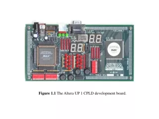
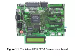
Introduction • Technology • Altera Quartus II • DE2 Development and Education Board
Design, fabrication and code • Processor Block Diagram/Schematic file • Operations symbols • 8bitadder, 8bitsupstract, 8bitand, 8bitor, 8bitnot, 8bitxor, 8bitnand, 8bitnor • Multiplexer symbols • Multiplexernot, Multiplexer, Multiplexer2, Multiplexerrez • HEXdec symbol • Converter symbol
HEXdec Input numbers Operations Multiplexers Output Displays Input pushbuttons Output LEDs Input selector switches Processor Block Diagram/Schematic file
Operations symbols • 8bitadderAddition is done with the useof two symbols:halfadder and fullader.
HALFADDER FULLADDER
Multiplexernot • There are two 8-bit numbers on the input and two selector pins (SEL0-SEL1) • There is one 8-bit number on the output. • The output number is eaqual to one of the input numbers depending of the selector pins.
HEXdec symbol • This symbol performs conversion of a binary number, which is at the input, into a decimal number which is displayed on the 7- segment displays. • There are 9 input and 49 output pins. • The conversion from binary to decimal numeral system is implemented using converter symbol. • Representation of a number onto 7-segment display is done with symbols HEX0-HEX9.
Converter symbol • This symbol is a graphical representation of converter.vhd file that is written in VHDL code. • This symbol does not only convert the number, but also it “determines” the distribution of digits in the decimal number. • There are 9 input pins and 29 output pins. • All commands are executed in a process (named CONVERSION) because they have to be executed sequentially (one by one).
Results in brief • Aquired knowlage about: • Elements and posibilities of DE2 Development and Education Board • Basics of VHDL (via converter.vhd) • Altera Quartus tools for synthesis and simulation • FPGAs
Conclusion • DE2 Developement and Education board advantages • FPGA advantages • VHDL advantages • Implementation: from lab demos to ESA projects
Thank you for your attention! Any questions?