Download

1 / 21
210 likes | 242 Views
Explore the design process for schematic or VHDL entry, connections of pushbuttons, LEDs, and FLEX device, active low OR-gate schematic examples, compilation, and timing analysis. Learn about jumper settings, VHDL and Verilog models, and CPLD placement using the Altera UP 1 board.

E N D
Design Compilation Simulation Verifcation GraphicalEntry Timing Diagram Program CPLD Compiler Timing Analysis UP 1 Development Board HDLEntry Figure 1.2 Design process for schematic or VHDL entry.
Figure 1.3 Connections between the pushbuttons, the LEDs, and the Altera FLEX device.
Figure 1.4 FLEX chip pin connection to seven-segment display decimal point.
Figure 1.5a and 1.5b. Equivalent circuits for ORing active low inputs and outputs.
Figure 1.6 Active low OR-gate schematic example with pinouts.
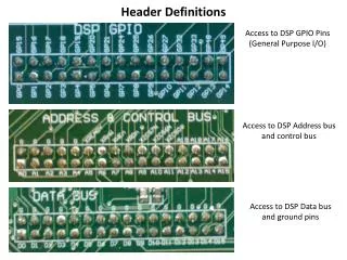
Device Pin Number Connections PB1 28 PB2 29 LED Decimal Point On the Left Seven-Segment Display 14 Table 1.1 Hardwired connections on the FLEX chip for the design.
Figure 1.7 Active low OR-gate schematic with pin numbers assigned.
Figure 1.10 ALTERA UP 1 board with jumper settings and PB1, PB2, and LED locations.
Table 1.2 Jumper settings for downloading to the MAX and FLEX devices.
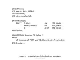
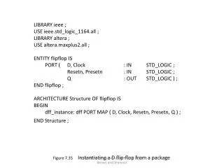
Figure 1.15 Verilog active low OR-gate model (with syntax error).
Figure 1.17 Timing analyzer showing input to output timing delays.
Figure 1.18 Floorplanner with internal CPLD placement of OR-gate logic cell and I/O pins.
ORGATE PB1 LED PB2 1 Figure 1.19 OR gate logic symbol.