
SEQUENTIAL CIRCUITS
E N D
Presentation Transcript
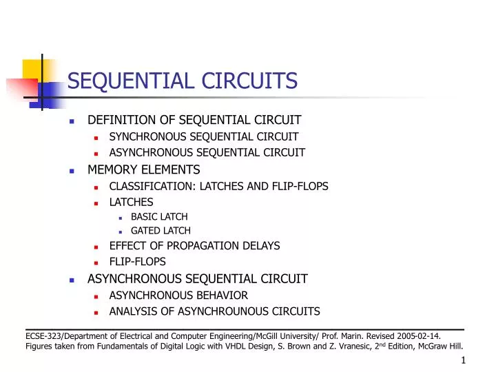
SEQUENTIAL CIRCUITS • DEFINITION OF SEQUENTIAL CIRCUIT • SYNCHRONOUS SEQUENTIAL CIRCUIT • ASYNCHRONOUS SEQUENTIAL CIRCUIT • MEMORY ELEMENTS • CLASSIFICATION: LATCHES AND FLIP-FLOPS • LATCHES • BASIC LATCH • GATED LATCH • EFFECT OF PROPAGATION DELAYS • FLIP-FLOPS • ASYNCHRONOUS SEQUENTIAL CIRCUIT • ASYNCHRONOUS BEHAVIOR • ANALYSIS OF ASYNCHROUNOUS CIRCUITS __________________________________________________ ECSE-323/Department of Electrical and Computer Engineering/McGill University/ Prof. Marin. Revised 2005-02-14. Figures taken from Fundamentals of Digital Logic with VHDL Design, S. Brown and Z. Vranesic, 2nd Edition, McGraw Hill.
DEFINITION OF SEQUENTIAL CIRCUIT • CIRCUITS IN WHICH THE VALUES OF THE OUTPUTS DEPENT ON: • THE PRESENT VALUES OF THE INPUTS • THE PAST BEHAVIOR OF THE CIRCUIT ARE CALLED SEQUENTIAL CIRCUIT. IN SUCH CIRCUITS STORAGE ELEMENTS STORE THE VALUES OF THE SIGNALS. THE CONTENTS OF THE STORAGE ELEMENTS REPRESENT THE STATE OF THE CIRCUIT. THERE ARE TWO TYPES: • SYNCHRONOUS, AND • ASYNCHRONOUS
W Combinational Combinational Z Flip-flops circuit circuit Q Clock DEFINITION OF SEQUENTIAL CIRCUIT SYNCHRONOUS SEQUENTIAL CIRCUITS: ARE SEQUENTIAL CIRCUITS CONTROLLED BY A CLOCK SIGNAL
R Y y Q S DEFINITION OF SEQUENTIAL CIRCUIT ASYNCHRONOUS SEQUENTIAL CIRCUITS: ARE SEQUENTIAL CIRCUITS: • WITH NO CLOCK SIGNALS, • NO FLIP-FLOPS TO STORE STATE VARIABLES • Feedback signal Gate-delay
Load A B A B Output Data TG1 TG2 MEMORY ELEMENTS EXAMPLES OF MEMORY ELEMENTS:
MEMORY ELEMENTS CLASSIFICATION: LATCHES AND FLIP-FLOPS BASIC LATCH: is a feedback connection of two NOR gates or two NAND gates. GATED LATCH: is a basic latch that includes input gating and a control input signal. FLIP-FLOPS: is a storage element based on the gated latch principle which can have its output statechanged only at the edge of the controlling clock signal.
MEMORY ELEMENTS CLASSIFICATION: LATCHES AND FLIP-FLOPS (Continues) • The state of the LATCH keeps changing according to the values of the input signals during the period when the clock is active. • The state of the FLIP-FLOP changes only at the edge of the controlling clock signal.
Q S R Q R a b Q a (no change) 0 0 0/1 1/0 0 1 0 1 1 0 1 0 1 1 0 0 Q b S (a) Circuit (b) Truth table t t t t t t t t t t 1 2 3 4 5 6 7 8 9 10 1 R 0 1 S 0 1 Q ? a 0 1 Q ? b 0 Time (c) Timing diagram MEMORY ELEMENTS LATCHES: BASIC LATCH
MEMORY ELEMENTS LATCHES: GATED RS LATCH
MEMORY ELEMENTS • LATCHES: GATED D LATCH
t su t h Clk D Q MEMORY ELEMENTS EFFECT OF PROPAGATION DELAYS: Latch Setup and hold times. SETUP TIME: Minimum time that the D input signal must be stable prior to the negative (positive) edge of the Clk (clock) signal. HOLD TIME: Minimum time that the D input signal must remain stable after the negative (positive) edge of the Clk (clock) signal
Master Slave Q Q m s Q Q D D Q D Clk Clk Q Q Q (a) Circuit Clock D Q m Q = Q s (b) Timing diagram Q D Q (c) Graphical symbol MEMORY ELEMENTS FLIP-FLOPS:They are storage elements that can change their state no more than once during one clock cycle. Two types: Master-Slave and Edge-triggered. • Master-Slave Flip-flop:
1 P3 P1 2 5 Q Clock 6 Q P2 3 Q D Clock Q (b) Graphical symbol 4 P4 D (a) Circuit MEMORY ELEMENTS FLIP-FLOPS (Continues). • Edge-triggered Flip-flop
MEMORY ELEMENTS • INPUT/OUTPUT BEHAVIOR OF LATCHES AND FLIP-FLOPS* _______________________________________ * Contemporary Logic Design by R.H. Katz, Benjamin Cummings, 1994, page 290.
Q D D Q a Clock Q Q Clk a Q D Q b Q Q b Q D Q c Q Q c Clock D Q a Q b Q c (b) Timing diagram MEMORY ELEMENTS • LEVEL-SENSITIVE VERSUS EDGE-TRIGGERED STORAGE ELEMENTS (a) Circuit
Q D !Q Clk > Q T !Q Clk > MEMORY ELEMENTS FLIP-FLOPS (Continues) CHARACTERISTIC AND EXCITATION EQUATIONS OF D, T AND J-K FLIP-FLOPS
MEMORY ELEMENTS FLIP-FLOPS (Continues) CHARACTERISTIC AND EXCITATION EQUATIONS OF D, T AND J-K FLIP-FLOPS J Q K !Q Clk > S Q R Clk !Q >
MEMORY ELEMENTS • FLIP-FLOPS (Continues) • FLIP-FLOP CONVERSIONS : Given a flip-flop as a buiding block, produce another type of flip-flop. • APPROACH: Determine the input logic to the given flip-flop by satisfying the condition that both flip-flops must have identical logic behavior (their outputs are the same)
MEMORY ELEMENTS • FLIP-FLOP CONVERSIONS (Continues): • Example: Produce the circuit of a J-K-type flip-flop using a T-type flip-flop as a building block and NAND gates as needed • The corresponding circuit is shown on next slide T = J !Q + K Q
MEMORY ELEMENTS • FLIP-FLOP CONVERSIONS: • Example (Continues): Circuit of a J-K flip-flop using a T flip-flop
ASYNCHRONOUS SEQUENTIAL CIRCUIT IN SYNCHRONOUS SEQUENTIAL CIRCUITS A CLOCK SIGNAL CONSISTING OF PULSES, CONTROLS THE STATE VARIABLES WHICH ARE REPRESENTED BY FLIP-FLOPS. THEY ARE SAID TO OPERATE IN PULSE MODE. IN ASYNCHRONOUS CIRCUITS STATE CHANGES ARE NOT TRIGGERED BY CLOCK PULSES. THEY DEPEND ON THE VALUES OF THE INPUT AND FEEDBACK VARIABLES. TWO CONDITIONS FOR PROPER OPERATION: 1.-INPUTS TO THE CIRCUIT MUST CHANGE ONE AT A TIME AND MUST REMAIN CONSTANT UNTIL THE CIRCUIT REACHES STABLE STATE. 2.-FEEDBACK VARIABLES SHOULD CHANGE ALSO ONE AT A TIME. WHEN ALL INTERNAL SIGNALS STOP CHANGING, THEN THE CIRCUIT IS SAID TO HAVE REACHED STABLE STATE. WHEN THE INPUTS SATISFY CONDITION 1 ABOVE, THEN THE CIRCUIT IS SAID TO OPERATE IN FUNDAMENTAL MODE.
R Y y Q S (a) Circuit with modeled gate delay ASYNCHRONOUS SEQUENTIAL CIRCUIT ASYNCHRONOUS BEHAVIOR Consider the Set-Reset latch. • The gates shown below have no delay. Their delay (twice one-gate delay) is represented by the square.
Next state Present SR = 00 state 01 10 11 y Y Y Y Y 0 0 0 1 0 1 1 0 1 0 (b) State-assigned table Figure 9.1. Analysis of the S-R latch. ASYNCHRONOUS SEQUENTIAL CIRCUIT ASYNCHRONOUS BEHAVIOR: Set-Reset latch (continues) • The circuit behavior is represented by a State-assigned table or Flow table which show every possible transition of the circuit for each input value. Stable-states are those circled in the table because, while the inputs are stable, present state is equal to next state (internal variables stop changing). Columns with no circled sates indicate circuit oscillation for that particular input value.
Next state Present Output state Q SR = 00 01 10 11 A A A B A 0 B B A B A 1 (a) State table SR 10 00 00 ¤ ¤ 01 A 0 B 1 10 11 01 11 (b) State diagram Figure 9.2. FSM model for the SR latch. MOORE MODEL ASYNCHRONOUS SEQUENTIAL CIRCUIT ASYNCHRONOUS BEHAVIOR: Set-Reset latch (continues) • FINITE-STATE-MACHINE MODEL: MOORE MODEL
Next state Output, Q Present state SR = 00 01 10 11 00 01 10 11 – A A A B A 0 0 0 – – B B A B A 1 1 SR/Q 10/ – 00/0 00/1 01/0 A B 10/1 11/0 ¤ 01 – ¤ 11 – ASYNCHRONOUS SEQUENTIAL CIRCUIT ASYNCHRONOUS BEHAVIOR: Set-Reset latch (continues) • FINITE-STATE-MACHINE MODEL: MEALY MODEL (a) State Table (b) State Diagram
ASYNCHRONOUS SEQUENTIAL CIRCUIT ANALYSIS OF ASYNCHROUNOUS CIRCUITS PROCEDURE: • CUT ALL FEEDBACK PATHS AND INSERT A DELAY ELEMENT AT EACH POINT WHERE CUT WAS MADE • INPUT TO THE DELAY ELEMENT IS THE NEXT STATE VARIABLE Yi WHILE THE OUTPUT IS THE PRESENT VALUE yi. • DERIVE THE NEXT-SATE AND OUTPUT EXPRESSIONS FROM THE CIRCUIT • DERIVE THE EXCITATION TABLE • DERIVE THE FLOW TABLE • DERIVE A STATE-DIAGRAM FROM THE FLOW TABLE
D Y y Q C (a) Circuit Next state Present CD = 00 state 01 10 11 y Y Y Y Y Q 0 0 0 0 1 0 1 1 1 0 1 1 (b) Excitation table Next state Present state CD = 00 01 10 11 Q A A A A B 0 B B B A B 1 (c) Flow table ASYNCHRONOUS SEQUENTIAL CIRCUIT • ANALYSIS OF ASYNCHROUNOUS CIRCUITS: EXAMPLE
Next state Present state CD = 00 01 10 11 Q A A A A B 0 B B B A B 1 (c) Flow Table 11 CD 0x 0x ¤ ¤ A 0 B 1 x0 x1 10 (d) State Diagram: Moore Model ASYNCHRONOUS SEQUENTIAL CIRCUIT • ANALYSIS OF ASYNCHROUNOUS CIRCUITS: EXAMPLE CONTINUES
ASYNCHRONOUS SEQUENTIAL CIRCUIT • SYNTHESIS OF ASYNCHROUNOUS CIRCUITS • THIS TOPIC IS NOT COVERED IN THIS COURSE. IT BELONGS TO A MORE ADVANCED LOGIC DESIGN COURSE. • THIS SUBJECT IS VERY IMPORTANT IN TODAYS DIGITAL SYSTEMS DESIGN BECAUSE CLOCKS ARE SO FAST THAT THEY PRESENT PROPAGATION DELAYS MAKING SUBSYSTEMS TO OPERATE OUT OF SYNCHRONIZATION. • TECHNIQUES FOR SYNTHESIS OF ASYNCHRONOUS CIRCUITS INCLUDE • THE HOFFMAN OR CLASSIC SYNTHESIS APPROACH • HANDSHAKING SIGNALING FOR TWO SUBSYSTEMS TO COMMUNICATE ASYNCHRONOUSLY