SEQUENTIAL CIRCUITS Introduction
SEQUENTIAL CIRCUITS Introduction. Overview. Circuits require memory to store intermediate data Sequential circuits use a periodic signal to determine when to store values. A clock signal can determine storage times Clock signals are periodic Single bit storage element is a flip flop

SEQUENTIAL CIRCUITS Introduction
E N D
Presentation Transcript
Overview Circuits require memory to store intermediate data Sequential circuits use a periodic signal to determine when to store values. A clock signal can determine storage times Clock signals are periodic Single bit storage element is a flip flop A basic type of flip flop is a latch Latches are made from logic gates NAND, NOR, AND, OR, Inverter
The story so far ... Logical operations which respond to combinations of inputs to produce an output. Call these combinational logic circuits. Usually these circuits do not contain loops However, some combinational circuits have loops:
The story so far ... Combinational circuits No way of remembering or storing information after inputs have been removed. To handle this, we need sequential logic capable of storing intermediate (and final) results.
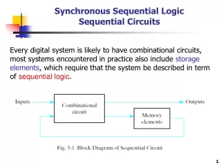
Sequential Circuits Combinational circuit Outputs Inputs Flip Flops Nextstate Presentstate Timing signal (clock) Clock a periodic external event (input) synchronizes when current state changes happen keeps system well-behaved makes it easier to design and build large systems
Cross-coupled Inverters • The system has two stable states • A stable value can be stored at inverter outputs • Not possible to set a desired state State 2 State 1
Cross-coupled Inverters (cont.) • This circuit has no stable states
S-R Latch with NORs R (reset) Q S R Q Q’ 0 0 Forbidden 1 1 1 0 0 1 0 0 1 0 Set 0 1 Reset Q 0 1 Stable S (set) 1 0 • S-R latch made from cross-coupled NORs • If Q = 1, set state • If Q = 0, reset state • Usually S=0 and R=0 • S=1 and R=1 generates unpredictable results set Q S R reset Q
S-R Latch with NORs R (reset) Q S R Q Q’ 0 0 Forbidden 1 1 1 0 0 1 0 0 1 0 Set 0 1 Reset Q 0 1 Stable S (set) 1 0
S-R Latch with NORs R (reset) Q S R Q Q’ 0 0 Forbidden 1 1 1 0 0 1 0 0 1 0 Set 0 1 Reset Q 0 1 Stable S (set) 1 0 • What happens if both inputs R and S simultaneously change from 0 to 1? • Race conditions
S-R Latch with NANDs S Q Q’ R S R Q Q’ 0 0 0 1 1 0 1 1 1 1 Forbidden 1 0 Set 0 1 Reset 0 1 Store 1 0 Latch made from cross-coupled NANDs Sometimes called S’-R’ latch Usually S=1 and R=1 S=0 and R=0 generates unpredictable results
NOR S-R Latch with Control Input Latch is level-sensitive, in regards to C Only stores data if C’ = 0 R’ Q C’ Q’ Latch operation enabled by C S’ Outputs change when C is low: RESET and SET Otherwise: HOLD Input sampling enabled by gates
S-R Latch with control input Occasionally, desirable to avoid latch changes C = 0 disables all latch state changes Control signal enables data change when C = 1 Right side of circuit same as ordinary S-R latch.
D Latch D X Y C Q Q’ D C Q Q’ 0 0 1 Q0 Q0’ Store 0 1 1 0 1 Reset 1 0 1 1 0 Set 1 1 1 1 1 Disallowed X X 0 Q0 Q0’ Store 0 1 0 1 1 1 1 0 X 0 Q0 Q0’ Q0 indicates the previous state (the previously stored value) X S Q C Q’ R Y
D Latch D C Q Q’ 0 1 0 1 1 1 1 0 X 0 Q0 Q0’ X S D Q C Q’ R Y Input value D is passed to output Q when C is high Input value D is ignored when C is low
D Latch x D Q z E C z Latches on following edge of clock E x Z only changes when E is high If E is high, Z will followX
D Latch x D Q z E C z Latches on following edge of clock E x The D latch stores data indefinitely, regardless of input D values, if C = 0 Forms basic storage element in computers
Enabling Signal x D Q z E C Complete the waveform
x D Q z E C Complete the waveform
Symbols for Latches SR latch is based on NOR gates S’R’ latch based on NAND gates D latch can be based on either. D latch sometimes called transparent latch
Notes Latches are based on combinational gates (e.g. NAND, NOR) Latches store data even after data input has been removed S-R latches operate like cross-coupled inverters with control inputs (S = set, R = reset) With additional gates, an S-R latch can be converted to a D latch (D stands for data) D latch is simple to understand conceptually When C = 1, data input D stored in latch and output as Q When C = 0, data input D ignored and previous latch value output at Q Next time: more storage elements!
Why FFs Latches respond to trigger levels on control inputs Example: If G = 1, input reflected at output Difficult to precisely time when to store data with latches Flip flips store data on a rising or falling trigger edge. Example: control input transitions from 0 -> 1, data input appears at output Data remains stable in the flip flop until until next rising edge. Different types of flip flops serve different functions Flip flops can be defined with characteristic functions.
Disadvantage of Transparent Latches Difficult to implement a shift register!
Clocking Event Positive edge triggered D Q C Q’ Hi-Lo edge Lo-Hi edge D C Q Q’ 0 0 1 1 1 0 X 0 Q0 Q0’ What if the output only changed on a C transition?
Master-Slave D Flip Flop Consider two latches combined together Only one C value active at a time Output changes on falling edge of the clock D C Q Q’ 0 1 0 1 1 1 1 0 X 0 Q0 Q0’
D Flip-Flop Positive edge triggered D Q C Q’ D C Q Q’ 0 0 1 1 1 0 X 0 Q0 Q0’ Stores a value on the positive edge of C Input changes at other times have no effect on output D gets latched to Q on the rising edge of the clock.
Clocked D Flip-Flop Stores a value on the positive edge of C Input changes at other times have no effect on output
Positive and Negative Edge D Flip-Flop Hi-Lo edge Lo-Hi edge D flops can be triggered on positive or negative edge Bubble before Clock (C) input indicates negative edge trigger
Positive Edge-Triggered J-K Flip-Flop J K CLK Q Q’ Created from D flop J sets K resets J=K=1 -> invert output 0 0 Q0 Q0’ 0 1 0 1 1 0 1 0 1 1 TOGGLE
Clocked J-K Flip Flop Two data inputs, J and K J -> set, K -> reset, if J=K=1 then toggle output Characteristic Table
T Q Q’ C 0 Q0 Q0’ 1 TOGGLE Positive Edge-Triggered T Flip-Flop Created from D flop T=0 -> keep current K resets T=1 -> invert current
Asynchronous Inputs • J, K are synchronous inputs • Effects on the output are synchronized with the CLK input. • Asynchronous inputs operate independently of the synchronous inputs and clock • Set the FF to 1/0 states at any time.
Asynchronous Inputs • Note reset signal (R) for D flip flop • If R = 0, the output Q is cleared • This event can occur at any time, regardless of the value of the CLK
Parallel Data Transfer Flip flops store outputs from combinational logic Multiple flops can store a collection of data
Notes Flip flops are powerful storage elements They can be constructed from gates and latches! D flip flop is simplest and most widely used Asynchronous inputs allow for clearing and presetting the flip flop output Multiple flops allow for data storage The basis of computer memory! Combine storage and logic to make a computation circuit Next time: Analyzing sequential circuits.
Must know items Understanding flip flop state: Stored values inside flip flops Clocked sequential circuits: Contain flip flops Representations of state: State equations State table State diagram Finite state machines Mealy machine Moore machine
Flip Flop State x D0 Q0 Q1 Q D Q’ y Q Q1 D Q0 Q’ D1 Clk y(t) = x(t)Q1(t)Q0(t) Q0(t+1) = D0(t) = x(t)Q1(t) Q1(t+1) = D1(t) = x(t) + Q0(t) Behavior of clocked sequential circuit can be determined from inputs, outputs and FF state
Output and State Equations x D0 Q0 Q1 Q D Q’ y Q Q1 D Q0 Q’ D1 Clk y(t) = x(t)Q1(t)Q0(t) Q0(t+1) = D0(t) = x(t)Q1(t) Q1(t+1) = D1(t) = x(t) + Q0(t) Next state dependent on previous state. Output equation State equations
State Table Sequence of outputs, inputs, and flip flop states enumerated in state table Present state indicates current value of flip flops Next state indicates state after next rising clock edge Output is output value on current clock edge Next State Output Present State x=0 x=1 x=0 x=1 0 0 0 1 1 0 1 1 00 10 0 0 10 10 0 0 00 11 0 0 10 11 0 1 Q1(t) Q0(t) Q1(t+1) Q0(t+1) State Table
State Table All possible input combinations enumerated All possible state combinations enumerated Separate columns for each output value. Sometimes easier to designate a symbol for each state. Next State Output Present State x=0 x=1 x=0 x=1 Let: s0 = 00 s1 = 01 s2 = 10 s3 = 11 s0 s1 s2 s3 s0s2 0 0 s2s2 0 0 s0s3 0 0 s2s3 0 1
State Diagram Circles indicate current state Arrows point to next state For x/y, x is input and y is output 1/1 11 Next State Output Present State x=0 x=1 x=0 x=1 0 0 0 1 1 0 1 1 00 100 0 10 100 0 00 110 0 10 110 1 0/0 0/0 0/0 00 01 10 1/0 1/0 0/0 1/0
1/1 0/0 0/0 0/0 s0 s1 s2 1/0 s3 0/0 1/0 1/0 State Diagram • Each state has two arrows leaving • One for x = 0 and one for x = 1 • Unlimited arrows can enter a state • Note use of state names in this example • Easier to identify
Flip Flop Input Equations Boolean expressions which indicate the input to the flip flops. x D0 Q0 Q1 Q D Q’ y Q Q1 D Q0 Q’ D1 Clk DQ0 = xQ1 DQ1 = x + Q0 Format implies type of flop used
Analysis with D Flip-Flops Identify flip flop input equations Identify output equation Note: this example has no output
Mealy Machine • Output based on state and present input Comb. Logic Comb. Logic Q(t+1) Flip Flops next state Q(t) Y(t) present state X(t) present input clk
Moore Machine • Output based on state only Comb. Logic Comb. Logic Y(t) Q(t+1) Flip Flops next state Q(t) present state X(t) present input clk
State Diagram with One Input & One Mealy Output Mano text focuses on Mealy machines State transitions are shown as a function of inputs and current outputs. e.g. 1 0/0 Input(s)/Output(s) shown in transition S1 1/0 1/1 S4 S2 0/0 0/0 0/0 1/0 S3 1/0

