Download

1 / 19
190 likes | 437 Views
Externally Tested Scan Circuit with Built-In Activity Monitor and Adaptive Test Clock. Priyadharshini Shanmugasundaram priyas@nvidia.com Vishwani D. Agrawal vagrawal@eng.auburn.edu Hyderabad, India, January 11, 2012. Testing of VLSI Circuits and Power.

E N D
Externally Tested Scan Circuit with Built-In Activity Monitor and Adaptive Test Clock PriyadharshiniShanmugasundaram priyas@nvidia.com Vishwani D. Agrawal vagrawal@eng.auburn.edu Hyderabad, India, January 11, 2012
Testing of VLSI Circuits and Power VLSI Design 2012 • High circuit activity during test leads to functional slowdown and high test power dissipation: • Peak power - Large IR drop in power distribution lines • Voltage droop and ground bounce (power supply noise) • Reduced voltage slows the gates down (delay fault) • Average power - Excessive heating • Timing failures • Permanent damage to circuit • Good chip may be labeled as bad → yield loss • Existing solution: Use worst-case test clock rate to keep average and peak power within specification. • Results in long test time.
Problem Statement VLSI Design 2012 • Reduce test time without exceeding the power specification: • Proposed solution: Adaptive test clock • Use worst-case clock rate when circuit activity is not known • Monitor circuit activity and speed up the clock when activity reduces
Previous Publications • P. Shanmugasundaram and V. D. Agrawal, “Dynamic Scan Clock Control in BIST Circuits,” RASDAT, January 2011. • P. Shanmugasundaram and V. D. Agrawal, “Dynamic Scan Clock Control in BIST Circuits,” Proc. 43rd IEEE Southeastern Symposium on System Theory, March 14-16, 2011, pp. 239-244. • P. Shanmugasundaram and V. D. Agrawal, “Dynamic Scan Clock Control for Test Time Reduction Maintaining Peak Power Limit,” Proc. 29th IEEE VLSI Test Symposium, May 2-4, 2011, pp. 248-253. • P. Shanmugasundaram, Test Time Optimization in Scan Circuits, Master’s Thesis, Department of ECE, Auburn University, Auburn, Alabama, December 2010. VLSI Design 2012
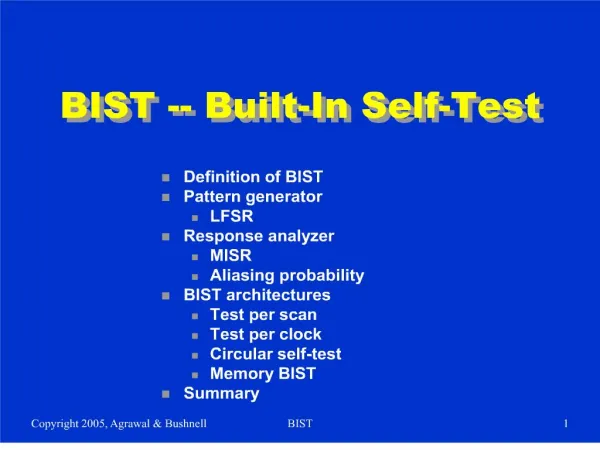
Built-In Self-Test (BIST) SR: Scanregister (flip-flops with dual inputs) RBG: Random bit generator 1 0 1 0 1 0 Combinational Logic Primary inputs Primary outputs Test multiplexers SR, RBG and RA have common clock and reset RA: Response analyzer VLSI Design 2012
RBG Generates 010101 SR: Scan register (flip-flops with dual inputs) RBG: Random bit generator 1 0 1 0 1 0 Primary inputs Primary outputs Test multiplexers SR, RBG and RA have common clock and reset RA: Response analyzer VLSI Design 2012
RBG Generates 111000 SR: Scan register (flip-flops with dual inputs) RBG: Random bit generator 0 0 0 1 1 1 Primary inputs Primary outputs Test multiplexers SR, RBG and RA have common clock and reset RA: Response analyzer VLSI Design 2012
Main Idea VLSI Design 2012 • Observation: Different sequences of test vector bits consume different amounts of power. • Conventional test clock frequency is chosen based on maximum test power consumption. • All test vector bits are applied with the same clock frequency. • Test vector bit sequences consuming lower power can be applied at higher scan clock frequencies without exceeding power budget of the chip.
Scan Clock Frequency • Upper bounds: • Maximum shift frequency allowed by shift register structure, F1 • Shift frequency determined by the highest scan activity and peak power budget, F2 • F1 >> F2 • Fixed scan clock: use F2 • Adaptive clock: monitor activity and vary clock frequency between F1 and F2 VLSI Design 2012
Speeding Up Scan Clock Power budget Cycle power Clock periods Power budget Cycle power Clock periods VLSI Design 2012
Monitoring Test Activity Non-transition monitor RBG: Random bit generator 1 0 1 0 1 0 Combinational Logic Primary inputs Primary outputs Test multiplexers SR, RBG and RA have common clock and reset RA: Response analyzer VLSI Design 2012
Monitoring Scan-in, VLSI Design 2012
Clock Rate vs. SR Activity N = number of flip-flops in scan shift register (SR) M = number of adjustable clock rates = 4, in this illustration F1 = fmax fmax/2 fmax/3 F2 = fmax/4 N N/2 N/4 0 Clock rate SSR transitions per clock 0 N/4 2N/4 3N/4 N Number of non-transitions counted VLSI Design 2012
Monitor Scan-out, VLSI Design 2012
Experimental Result - • ATPG pattern sets, generated by Tetramax, for four large benchmark circuits analyzed for trends in peak activity factor • Mean () • Standard deviation () • Peak activity factor was lower than 0.65 in vector sets of all large benchmark circuits
Externally Tested Circuit VLSI Design 2012 • Advantest T2000GS Automatic Test Equipment (ATE) • Start scan-in assuming for captured state • Results for ITC02 benchmark t512505 • N = 76,714 flip-flops (full-scan) • Scan clock frequency steps, v = 512 • Reference case scan clock frequency determined for activity , assumed 100kHz
Adaptive Clock Testing VLSI Design 2012 • ATE supplies 51.2 MHz test clock • Test for stuck-at faults • DUT with monitoring and clock control implemented in FPGA • Synchronizer implemented in FPGA as a vector buffer, working with 51.2MHz clock • Adaptive clock: • Begin scan-in with 100kHz scan clock. Set counter. • Step up frequency when count of non-transitions entering scan chain is . Set counter. • Step down frequency when count of non-transitions leaving scan chain is . Set counter.
Test Time Reduction (%) in t512505 VLSI Design 2012
Conclusion VLSI Design 2012 • Dynamic control of scan clock frequency proposed: • Reduces testing time without exceeding power budget. • On-chip activity monitor for self testing circuits keeps track of activity in scan chain and adjusts scan clock rate. • On-chip or off-chip activity monitor can be used for externally tested circuits. • Hand-shake protocol used for communication between ATE and DUT. • Vectors with low average scan-in activity and high peak activity achieve large reduction in test time. • Method can be implemented in circuits using compression hardware • Activity monitored at every internal scan chain. • Up to 50% reduction in test time achieved in circuits when start frequency not pre-determined • Results more significant when start frequency is pre-determined.