Download
1 / 83
1.23k likes | 2.38k Views
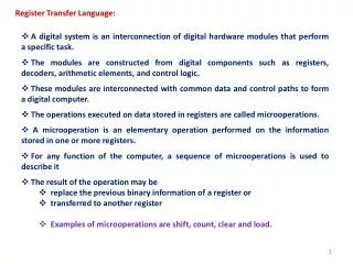
Register Transfer Language:. A digital system is an interconnection of digital hardware modules that perform a specific task. The modules are constructed from digital components such as registers, decoders, arithmetic elements, and control logic.

E N D
Register Transfer Language: • A digital system is an interconnection of digital hardware modules that perform a specific task. • The modules are constructed from digital components such as registers, decoders, arithmetic elements, and control logic. • These modules are interconnected with common data and control paths to form a digital computer. • The operations executed on data stored in registers are called microoperations. • A microoperation is an elementary operation performed on the information stored in one or more registers. • For any function of the computer, a sequence of microoperations is used to describe it • The result of the operation may be • replace the previous binary information of a register or • transferred to another register • Examples of microoperations are shift, count, clear and load.
Register Transfer Language: • The internal hardware organization of a digital computer is defined by specifying: • The set of registers it contains and their function. • The sequence of microoperations performed on the binary information stored in the registers. • The control that initiates the sequence of microoperations. • The symbolic notation used to describe the microoperation transfers among registers is called a register transfer language. • The term register transfer implies the availability of hardware logic circuit that can transfer the result of the operation to the same or another register. • A register transfer language (RTL) is a system for expressing in symbolic form the microoperation sequences among the register of a digital module. • Computer registers are designated by capital letters (sometimes followed by numerals) to denote the function of the register • R1: processor register (general purpose register) • MAR: Memory Address Register (holds an address for a memory unit) • PC: Program Counter • IR: Instruction Register • SR: Status Register
Register Transfer: • The individual flip-flops in an n-bit register are numbered in sequence from 0 to n-1 (from the right position toward the left position). 15 0 PC Numbering of bits • Information transfer from one register to another is described by a replacement operator: • R2 ← R1 • This statement denotes a transfer of the content of register R1 into register R2. • The transfer happens in one clock cycle. • The content of the R1 (source) does not change. • The content of the R2 (destination) will be lost and replaced by the new data transferred from R1. R1 7 6 5 4 3 2 1 0 15 0 8 7 Showing individual bits Register R1 Upper byte PC(H) PC(L) Lower byte Partitioned into two parts
Register Transfer: • Register transfer statement implies that the circuits are available from the outputs of the source register to the inputs of the destination register, and that the destination register has a parallel load capability. • Conditional transfer occurs only under a control condition • This can be shown by means of an if-then statement: • If (P = 1) then (R2 ← R1) • where P is control signal generated in the control section. • The control variables are separated from the register transfer operation by specifying a control function. • A control function is a Boolean variable that is equal to 1 or 0. • The control function is included in the statement as follows: • P: R2 ← R1 • The control condition is terminated with a colon. • It symbolizes that the transfer operation takes place by the hardware only if P = 1.
Register Transfer: Control Circuit P Load Clock R2 n Block Diagram: R1 t t+1 Clock Synchronized with the clock Load Transfer occurs here Timing Diagram:
Register Transfer: • The statement • T: R2 ← R1, R1 ← R2 • denotes an operation that exchanges the contents of two registers during one common clock pulse provided that T = 1. • This simultaneous operation is possible with registers that have edge-triggered flip-flops. Basic Symbols for Register Transfer:
Bus and Memory Transfers: • A typical digital computer has many registers, and paths must be provided to transfer information from one register to another. • The number of wires will be excessive if separate lines are used between each register and all other registers in the system. • The more efficient scheme for transferring information between registers in a multiple-register system is a common bus system. • A bus structure consists of a set of common lines, one for each bit of a register, through which binary information is transferred one at a time. • Control signals determine which register is selected by the bus during each particular register transfer. • Common bus system can be constructed either by using multiplexers or by using three-state buffers.
Bus System for Four Registers using Multiplexers: S1 S0 • BUS ← C • R1 ← BUS • R1 ← C 4-line common bus Register D Register C Register B Register A • A bus system will multiplex k registers of n bits each to produce an n-line common bus. • The number of multiplexers needed to construct the bus is equal to n, the number of bits in each register. • The size of each multiplexer must be k X 1, since it multiplexes k data lines.
Bus System for Four Registers using Three-State Buffers: • A three state gate is a digital circuit that exhibits three states. • Logic 1 State • Logic 0 State • High Impedance State Z (Open Circuit) • Buffer --- A device designed to be inserted between other devices to match impedance, to prevent mixed interactions, and to supply additional drive or relay capability • Buffer types are classified as inverting or non-inverting. Normal input A If C=1, Output Y = A If C=0, Output = High-impedance Control input C
Bus System for Four Registers using Three-State Buffers: A0 Bus line for bit 0 B0 C0 D0 Select inputs Enable input • The outputs of four buffer are connected together to form a single bus line. • No more than one buffer may be in the active state at any given time. Memory Transfer: AR: Address Register. DR: Data Register. M : Memory Word (Data) • Memory Read : A transfer information into DR from the memory word M selected by the address in AR • Memory Write : A transfer information from R1 into the memory word M selected by the address in AR
Microoperations: • A microoperation is an elementary operation performed with the data stored in registers. • The microoperations performed in digital systems are classified into four categories: • Register transfer microoperations --- transfer binary information one register to another. • Arithmetic microoperations --- perform arithmetic operation on numeric data stored in registers. • Logic microoperations --- perform bit manipulation operations on numeric data stored in registers. • Shift microoperations --- perform shift operations on data stored in registers.
4-bit Binary Adder: B3 A3 B2 A2 B1 A1 B0 A0 C3 C2 C1 C0 S0 S2 S1 S3 C4
4-bit Binary Adder-Subtractor: B3 A3 B2 A2 B1 A1 B0 A0 M C2 C1 C3 C0 C4 S3 S2 S1 S0
4-bit Binary Adder-Subtractor: M = 0 M = 1 A - B A + B
4-bit Binary Incrementer: A3 A2 A1 A0 1 C4 S3 S2 S1 S0
Cin Arithmetic Circuit: S0 S1 A0 B0 A1 B1 A2 B2 A3 B3 0 D0 D1 D2 D3 A+B’=A+B’+1-1 = A-B-1 A+1111=A-1 A-1+1=A Cout
Logic Microoperations: • Logic microoperations specify binary operations for strings of bits stored in registers. • These operations consider each bit of the register separately and treat them as binary variables. • Example: • 1010 Content of R1 • + 1100 Content of R2 • 0110 Content of R1 after P=1 • Special Symbols • Special symbols will be adopted for the logic microoperations OR(V), AND(Ʌ), and complement (a bar on top), to distinguish them from the corresponding symbols used to express Boolean functions.
Logic Microoperations: Logic OR Arithmetic ADD Ai Bi
List of Logic Microoperations: • There are 16 different logic microoperations that can be performed with two binary variables, determined from all possible truth tables obtained with two binary variables, as shown below: • The 16 Boolean functions of two variables x and y are expressed in algebraic form in the first column of table #.
Logic Microoperations --- Applications: • Logic microoperations are very useful for manipulating individual bits or a portion of a word stored in a register • Used to change bit values, delete a group of bits, or insert new bit values • Selective-set • The selective-set operation sets to 1 the bits in register A where there are corresponding 1’s in register B. It does not effect bit positions that have 0’s in B. • 1010 A before • 1100 B(Logic Operand) • 0110 A After • 1010 A before • 1100 B(Logic Operand) • 1110 A After • Selective-complement • The selective-complement operation complements bits in A where there are corresponding 1’s in B. It does not effect bit positions that have 0’s in B.
Logic Microoperations --- Applications: • Selective-clear • The selective-clear operation clears to 0 the bits in A only where there are corresponding 1’s in B. • 1010 A before • 1100 B(Logic Operand) • 1000 A After masking • Selective-mask • The mask operation is similar to the selective-clear operation except that the bits of A are cleared only where there are corresponding 0’s in B. • 1010 A before • 1100 B(Logic Operand) • 0010 A After 0110A 0110B 0000 A after clear • Clear • The clear operation compares the words in A and B and produces an all 0’s result if the two numbers are equal
Shift Microoperations: • Used for serial transfer of data. • Three types of shift: Logical, Circular, and Arithmetic.
Logical Shift: • Transfers 0 through the serial input. Logical Shift Left: Logical Shift Right: R0 R0 Rn-1 Rn-1 R3 R3 R2 R2 R1 R1 ? 0 ? 0
Circular Shift: • Also known as rotate operation, circulates the bits of the register around the two ends without loss of information. • This is accomplished by connecting the serial output of the shift register to its serial input. R0 R0 Rn-1 R3 Rn-1 R3 R2 R1 R2 R1 Circular Shift Left Circular Shift Right
Circular Shift Examples: Arithmetic Shift: • Shifts a signed binary number to the left or right. • An arithmetic shift-left multiplies a signed binary number by 2: • ashl (00100): 01000 • An arithmetic shift-right divides the number by 2: • ashr (00100) : 00010
Arithmetic Shift Right: R0 Rn-1 R3 R2 R1 ? Sign Bit Arithmetic Shift Right
Arithmetic Shift Left: • The arithmetic shift-left inserts a 0 into R0, and shifts all other bits to the left. • The initial bit of R n – 1 is lost and replaced by the bit from R n – 2. R0 Rn-1 R3 R2 R1 0 ? Sign Bit Arithmetic Shift Left
Arithmetic Shift Left: • A sign reversal occurs if the bit in Rn-1 changes in value after the shift. • This happens if the multiplication by 2 causes an overflow. • An overflow flip-flop VS can be used to detect an arithmetic shift-left overflow. • VS = Rn-1 Rn-2 Rn-1 1 overflow 0 no overflow VS= Rn-2
Arithmetic Shift Unit: A1 A2 Serial Input IL Serial Input IR A3 A0 Select 0 for shift right 1 for shift left 0 0 0 0 S 1 S 1 S 1 S 1 MUX MUX MUX MUX H3 H2 H1 H0
Arithmetic Logic Shift Unit: S3 S2 S1 S0 Ci Di C i + 1 Fi Bi Ei Ai A i - 1 A i + 1
Instruction Codes: • The internal organization of a digital system is defined by the sequence of microoperations it performs on data stored in the registers. • The user of a program can control the process by means of a program. • A program is a set of instructions that specify the operations, operands, and the sequence by which processing has to occur. • An instruction code is a group of bits that instruct that the computer to perform a specific operation. • An instruction code is usually divided into two parts, operation code (opcode) and operand. • The operation code is a group of bits that define such operations as add, subtract, multiply, shift, and compliment. • A computer operation is a part of an instruction stored in computer memory that tells the computer to perform a specific operation, which requires a sequence of microoperations in internal computer registers. • An operation code is sometimes called a macrooperation because it specifies a set of micro-operations.
Stored Program Organization: • A stored program organization consists of one processor register and an instruction code format with two parts. • The first part specifies the operation to be performed and the second specifies an address. • The memory address tells the control where to find an operand in memory. • Instructions are stored in one section of memory and data in another. Memory 4096 X 16 15 12 11 0 Instruction (program) Opcode Address Instruction Format Operands (data) 15 0 Binary operand (Data) Processor register (accumulator or AC)
Stored Program Organization: • When the second part of an instruction code specifies an operand (not an address), the instruction is said to have an immediate operand. • When the second part specifies the address of an operand, the instruction is said to have direct address. • When the second part of an instruction code specifies an address of a memory word in which the address of the operand is found, the instruction is said to have indirect address. 15 14 12 11 0 I Opcode Address Instruction Format • Instruction code format that consists of a 3-bit operation code, a 12-bit address, and a address mode bit designated by I. • The mode bit is 0 for a direct address and 1 for an indirect address. • The effective address is the address of the operand in a computation-type instruction or the target address in a branch-type instruction.
Stored Program Organization: Memory Memory 22 0 ADD 457 35 1 ADD 300 300 1350 15 14 12 11 0 457 Operand I Opcode Address 1350 Operand Instruction Format + + AC AC Indirect address Direct address
Basic Computer Registers and Memory: 15 0 IR Memory 4096 words 16 bits per word 15 0 15 0 TR DR 15 0 11 0 11 0 7 0 7 0 AC OUTR AR PC INPR
Computer Registers: Common Bus System: • The basic computer has eight registers, a memory unit, and a control unit. • Paths must be provided to transfer information from one register to another and between memory and registers. • A more efficient scheme for transferring information in a system with many registers is to use a common bus.
Common Bus System: • The outputs of seven registers and memory are connected to the common bus. • The specific output is selected by MUX (S0, S1, S2) : • Memory(7), AR(1), PC(2), DR(3), AC(4), IR(5), TR(6) • When LD(Load Input) is enable, the particular register receives the data from the bus • Control Input : LD, INC, CLR, Write, Read • Load input (LD): Enables the input of a register to download bits form the common bus. When LD = 1 for a register, the data on the common bus is read into the register during the next clock pulse transition. • Increment input (INR): Increments the content of a register. • Clear input (CLR): Clear the content of a register to zero.
Common Bus System: s0 s1 s2 Bus Memory Unit 4096x16 7 Address WRITE READ 1 AR CLR LD INR 2 PC CLR LD INR 3 DR LD CLR INR E Adder & Logic 4 AC LD CLR INR INPR 5 IR LD TR 6 INR CLR LD OUTR Clock LD 16-bit common bus
Computer Instructions: • The basic computer has three instruction formats: • Memory – reference instructions • Register – reference instructions • Input – output instructions 15 14 12 11 0 (Opcode = 000 through 110) I Opcode Address Memory – reference instruction 15 12 11 0 0 1 1 1 Register Operation (Opcode = 111, I = 0) Register - reference instruction 15 12 11 0 1 1 1 1 I/O Operation (Opcode = 111, I = 1) Input – output instruction
Assembly Language Program to Add Two Numbers: • The numbers may be positive or negative, but if negative, they must be converted to binary in the signed 2’s compliment representation. • The symbols ORG, DEC, and END are called as pseudo instructions.
Program Control: • Program Control Instruction: Branch and Jump instructions are used interchangeably to mean the same thing. • Status register bits: 8 8 C7 8-bit ALU C8 F7 – F0 V Z S C F7 Check for zero output 8 Output F
Program Control: • Status Bit Conditions: • A status register stores status bit conditions called condition-code bits or flag bits • The bits are set or cleared as a result of an operation performed in the ALU. • 4-bit status register • Bit C (carry) is set to 1 if the end carry C8 is 1. • Bit S (sign) is set to 1 if the highest-order bit F7 is 1. • Bit Z (zero) is set to 1 if the output of the ALU contains all 0’s. • Bit V (overflow) is set to 1 if the exclusive-OR of the last two carries (C8 and C7) is equal to 1. Example : A - B = A + ( 2’s Comp. of B ) : A =11110000, B = 00010100 • 11110000 • + 11101100 (2’s comp. of B) • 1 11011100 C = 1, S = 1, V = 0, Z = 0
Program Interrupt: • Program Interrupt • Transfer program control from a currently running program to another service program as a result of an external or internal generated request. • Control returns to the original program after the service program is executed. • Interrupt Service Program: • An interrupt is initiated by an internal or external signal (except for software interrupt). • The address of the interrupt service program is determined by the hardware. • An interrupt procedure stores all the information necessary to define the state of the CPU.
Program Interrupt: External Int. Internal Int. Software Int. PC, CPU Register, Status Register, (PSW)