MOSFET operation
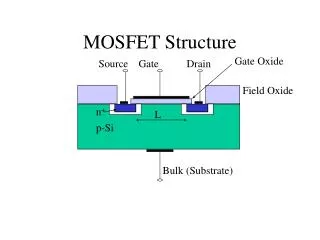
MOSFET operation. Animation of the MOSFET manufacturing process I encourage you to look at the website given below and use the button “animate to next” – the actual process is described for each step. http://jas.eng.buffalo.edu/education/fab/NMOS/nmos.html. Basic structure of the MOSFET.


MOSFET operation
E N D
Presentation Transcript
Animation of the MOSFET manufacturing processI encourage you to look at the website given below and use the button “animate to next” – the actual process is described for each step. http://jas.eng.buffalo.edu/education/fab/NMOS/nmos.html
V G MOS capacitor p type semiconductorvoltage bias effects –battery switched + + + + E - + - + - + - +
V G MOSFET p type semiconductor gate voltage VG > VT Electrons can flow from the source to the drain
L is not between the metal electrodes
V G NMOS -- p type semiconductor -- gate voltage VG variable - circuit models Enhancement mode Depletion mode n channel
V G PMOS -- n type semiconductor -- gate voltage VG variable - circuit models Enhancement mode Depletion mode p channel
NMOS & PMOS NMOS – n channel in a p-type semiconductor PMOS – p channel in an n-type semiconductor - +
V G NMOS -- p type semiconductor -- gate voltage VGS < VT -
V G NMOS -- p type semiconductor -- gate voltage VGS > VT - -
V G Derivation of the conductance
V G NMOS -- p type semiconductor -- gate voltage VGS > VT – long channel
V G NMOS -- p type semiconductor – VGS > VT & changing VDS
Biasing effects N channel MOSFEThttp://www.mtmi.vu.lt/pfk/funkc_dariniai/transistor/mosfet.htm