MOSFET
Introduction to Metal-Oxide-Semiconductor Field Effect Transistors (MOSFETs) Chapter 7, Anderson and Anderson. MOSFET. History Structure Review Future Threshold Voltage I-V Characteristics Modifications to I-V: Depletion layer correction (Sup. 3) Mobility, Vsat Short Channel Effects


MOSFET
E N D
Presentation Transcript
Introduction toMetal-Oxide-SemiconductorField Effect Transistors(MOSFETs)Chapter 7, Anderson and Anderson
MOSFET • History • Structure • Review • Future • Threshold Voltage • I-V Characteristics • Modifications to I-V: • Depletion layer correction (Sup. 3) • Mobility, Vsat • Short Channel Effects • Channel Length Modulation • Channel Quantum Effects • MOSFET Scaling and Current Topics (Literature + Sup. 3) • Subthreshold Behavior • Damage and Temperature (Sup. 3) • Spice (Sup. 3) • HFET, MESFET, JFET, DRAM, CCD (Some in Sup. 3)
MOSFET History (Very Short!) • First Patents: • 1935 • Variable Capacitor Proposed: • 1959 • Silicon MOS: • 1960 • Clean PMOS, NMOS: • Late 1960s, big growth! • CCDs: • 1970s, Bell Labs • Switch to CMOS: • 1980s
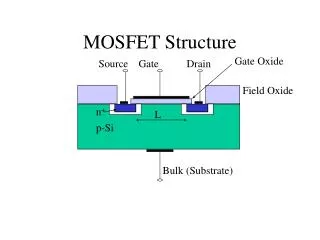
gate: metal or heavily doped poly-Si G body B source S drain D metal oxide p n+ n+ W L Structure: n-channel MOSFET(NMOS) IG=0 (bulk or substrate) ID=IS y IS x
D G B (IB=0, should be reverse biased) S Circuit Symbol (NMOS)enhancement-type: no channel at zero gate voltage ID= IS IG= 0 G-Gate D-Drain S-Source B-Substrate or Body IS
gate: metal or heavily doped poly-Si G body B source S drain D metal oxide p n+ n+ W L Structure: n-channel MOSFET(NMOS) IG=0 (bulk or substrate) ID=IS y IS x
Energy bands (“flat band” condition; not equilibrium) (equilibrium)
gate G body B source S drain D + - n++ oxide p n+ n+ W L Flatbands! For this choice of materials, VGS<0n+pn+ structure ID ~ 0 VGS VD=Vs
gate G body B source S drain D + - n++ oxide p n+ n+ W L Flatbands < VGS < VT (Includes VGS=0 here).n+-depletion-n+ structure ID ~ 0 VD=Vs +++
gate G body B source S drain D + - VD=Vs +++ +++ +++ n++ oxide p n+ n+ - - - - - W L VGS > VTn+-n-n+ structure inversion
Channel Charge (Qch) VGS>VT Depletion region charge (QB) is due to uncovered acceptor ions Qch
n++ p n+ n+ W L (x) Ec(y) with VDS=0
Increasing VGS decreases EB EB EF ~ EC y 0 L
B S D + - +++ VGS1>Vt +++ metal oxide p n+ - - - - n+ Triode Region A voltage-controlled resistor @small VDS ID increasing VGS B S D - + +++ VGS2>VGS1 +++ +++ G metal oxide p n+ n+ - - - - - - VDS cut-off B 0.1 v S D + - +++ VGS3>VGS2 +++ +++ Increasing VGS puts more charge in the channel, allowing more drain current to flow +++ metal oxide p n+ - - - - - - - - - n+
gate G body B source S + drain D - VDS large +++ +++ +++ metal oxide p n+ n+ Saturation Regionoccurs at large VDS As the drain voltage increases, the difference in voltage between the drain and the gate becomes smaller. At some point, the difference is too small to maintain the channel near the drain pinch-off
gate G body B source S + drain D - VDS large +++ +++ +++ metal oxide p n+ n+ Saturation Regionoccurs at large VDS The saturation region is when the MOSFET experiences pinch-off. Pinch-off occurs when VG - VD is less than VT.
gate G body B source S + drain D - VD>>Vs +++ +++ +++ metal oxide p n+ n+ Saturation Regionoccurs at large VDS VGS - VDS < VT or VGD < VDS > VGS - VT VT
Saturation Regiononce pinch-off occurs, there is no further increase in drain current saturation ID triode VDS>VGS-VT increasing VGS VDS<VGS-VT VDS 0.1 v
Simplified MOSFET I-V Equations Cut-off: VGS< VT ID = IS = 0 Triode: VGS>VT and VDS < VGS-VT ID = kn’(W/L)[(VGS-VT)VDS - 1/2VDS2] Saturation: VGS>VT and VDS > VGS-VT ID = 1/2kn’(W/L)(VGS-VT)2 where kn’= (electron mobility)x(gate capacitance) = mn(eox/tox) …electron velocity = mnE and VT depends on the doping concentration and gate material used (…more details later)
gate: metal or heavily doped poly-Si G body B source S drain D metal oxide p n+ n+ W L Structure: n-channel MOSFET(NMOS) IG=0 (bulk or substrate) ID=IS y IS x
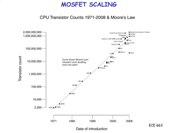
MOSFET Future (One Part of) • International Technology Roadmap for Semiconductors, 2008 update. • Look at size, manufacturing technique.
MOSFET Scaling ECE G201
Gate prevents “top” gate Fin (30nm) BOX
Energy bands (“flat band” condition; not equilibrium) (equilibrium)
Channel Charge (Qch) VGS>VT Depletion region charge (QB) is due to uncovered acceptor ions Qch
Threshold Voltage Definition VGS = VT when the carrier concentration in the channel is equal to the carrier concentration in the bulk silicon. Mathematically, this occurs when fs=2ff , where fsis called the surface potential