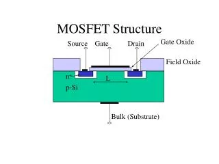
MOSFET Device Structure
MOSFET Device Structure. Semiconductor Equations. Poisson Equation:. Electron current continuity equation:. Hole current continuity equation:. Electron current equation:. Hole current equation:. MOSFET Device Simulation. Converged?. Iterative Gummel Block Method. Solve for f , n, p.


MOSFET Device Structure
E N D
Presentation Transcript
MOSFET Device Structure Semiconductor Equations Poisson Equation: Electron current continuity equation: Hole current continuity equation: Electron current equation: Hole current equation: MOSFET Device Simulation
Converged? Iterative Gummel Block Method. Solve for f, n, p Discretization of the semiconductor equations Newton’s Method for better accuracy Set up the device dimensions, material properties, temperature, bias voltages, doping profile, etc. Initial Guess for f, fn and fp Current Continuity? Extract f, electron and hole concentrations, mobility, current density, IV characteristics, etc. Simulation Methodology Y N N Y
Low field mobility: Oxide Matthiessen's rule Electron Flow Bulk mLF = Low Field Mobility mB = Bulk Mobility mSP = Surface Phonon Mobility mSR = Surface Roughness mobility mC = Trapped interface charge mobility Electron Surface Phonon Trap Surface Roughness Fixed Charge High field mobility: Mobility Models High Field Mobility:
Caughey – Thomas Model for bulk mobility: Temperature dependence: Doping dependence: Surface Phonon Mobility: tac = Surface acoustic phonon relaxation time E┴ = Perpendicular E. Field an, bn = calculated from phonon scattering equation
Surface Roughness Mobility: rSR = Surface roughness parameter. Higher the value ofrSR, smoother is the surface and lesser is the degradation in total mobility Interface Trap Charge Mobility: Corresponds to effect of coulomb scattering of mobile charged carriers by fixed charge and interface trap charge. The term also accounts for the screening of these charges by electrons at strong inversion. nf = Fixed oxide charge ne = Inversion layer electron concentration screen_fit, screen_factor = fitting parameters for the screening effect Nit = Occupied interface trap density atemp = Temperature dependence Git = from Coulomb Scattering model
4H SiC 200mm x 200mm MOSFET: Id-Vgs Simulation Fit at T=27oC
4H SiC 200mm x 200mm MOSFET: Id-Vds Simulation Fit at T=27oC
Bulk Mobility …. Bulk mobility at Room Temperature and D ~ 1015 is 4H SiC: ~ 800 cm2/Vs 6H SiC: ~ 400 cm2/Vs
Effect of surface roughness is negligible as compared to the effect of interface traps on the total mobility. Surface Roughness Mobility …. 4H rSR Value is taken from Linewih (2002) paper
Dit = Density of traps per unit energy f(E) is the probability density function. It is directly proportional to the mobile charge concentration (ne). Hence as MOSFET goes towards stronger inversion, the occupied interface trap density increases. Occupied interface trap density (Nit) 4H SiC has a higher bandgap than 6H SiC (by 0.2eV). Ditedge value for 4H SiC is obtained by extrapolating the Dit-E curve for 6H SiC by 0.1eV. This gives a very high Ditedge value for 4H SiC because of the exponential relation between Dit and E near the band edge. Hence 4H SiC has much higher interface traps than 6H SiC.
Extrapolation of Dit-E curve for 6H SiC to get Dit-E characteristics for 4H SiC Final Dit-E curve for 4H that is used: Dit_edge = 2.15 x 1013 cm-2eV-1 Dit_mid = 6.5 x 1011 cm-2eV-1
Occupied interface trap density increases with increase in Vgs. This is because the inversion layer electron concentration increases with increase in Vgs causing more traps to get filled Nit vs. position for different Vgs. T=27oC Device: 4H SiC MOSFET W/L: 200 mm / 200 mm Bias: Vgs = 2 to 4V Vds = 4V
Occupied interface trap density decreases with increase in temperature because trapped electrons can escape by gaining sufficient energy at higher temperatures. So as the temperature increases, effect of interface trap charge decreases, increasing overall mobility Nit vs. position for different Temperatures Device: 4H SiC MOSFET W/L: 200 mm / 200 mm Bias: Vgs = 6V Vds = 1V
The change in Id values for a tenfold improvement of the surface roughness factor, is very small at all three temperatures. Thus surface roughness does not change the current with change in temperature. The increase in current with temperature is caused by the reduction of filled interface trap density as temperature increases. Comparing effects of Surface Roughness and Interface traps at different Temperatures Device: 4H SiC MOSFET W/L: 200 mm / 200 mm Bias: Vgs = 6V Vds = 0-8V
Future Work… • Better screening model based on Brooks-Herring ionized impurity scattering model • Surface roughness calculation to get proper value for rSR • Fitting data at higher temperatures • High power MOSFET simulation • Investigating gate leakage in SiC MOSFETs • Building a Graphical User Interface for the simulator