MOSFET Scaling
MOSFET Scaling. ECE G201. next. Most Simple Model: Constant Field Scaling. E = V DD /L after scaling becomes E = (V DD / a )/(L/ a ) …where a >1. Impurity Concentration Scaling must also follow length scaling for depletion widths.


MOSFET Scaling
E N D
Presentation Transcript
MOSFET Scaling ECE G201
next Most Simple Model: Constant Field Scaling E = VDD/L after scaling becomes E = (VDD/a)/(L/a) …where a>1
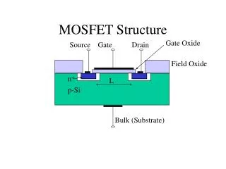
Impurity Concentration Scalingmust also follow length scaling for depletion widths Recall, that the source and drain are heavily doped and therefore the junctions are one-sided (n+p for NMOS): W = (2eVDD/qNA)1/2 …unscaled FET W/a = (2eVDD / a2qNA)1/2 = [2e(VDD/a)/qaNA]1/2 Therefore, the doping levels must increase by a factor a if the depletion widths are to scale down.
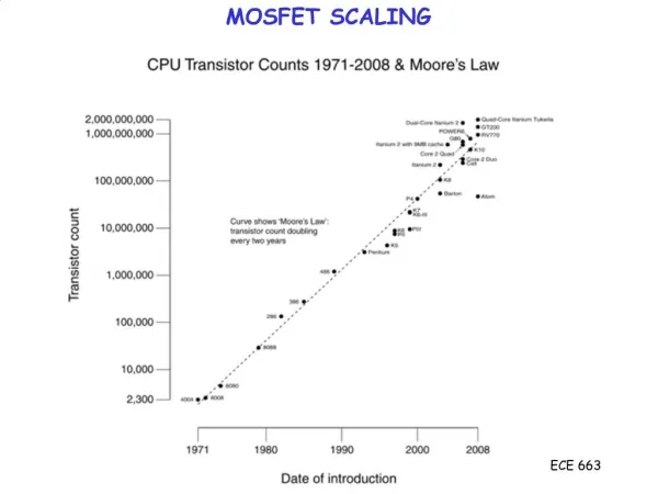
Historical Scaling“Moore’s Law:” number of transistors/chip doubles every 18 mo. 1 generation: ~18 mo. L decreases by 0.65/generation (a = 1/0.65 = 1.5) VDD decreases by 0.85/generation Therefore, constant field scaling (VDD/L) is not strictly followed.
Generalized Scaling Length: a = 1/0.65 = 1.5 Voltage: b = 1/0.85 = 1.2 Electric field:E increases x1.25 Doping: ba = x1.8 (!) note: not strictly followed
EC EV W Junction Leakage CurrentTunneling current due to highly doped Drain-Body junctions B D IJE Recall: tunneling T = Kexp(-2kW)
Gate Leakage Currenttox 0 means large tunneling current A large oxide capacitance is needed to control the channel charge and subthreshold current: Vch = VGS(Cox’+CB’)/Cox’ …where Cox’ = eox/tox since tox is limited by tunneling, research is focused on alternate gate dielectric materials with larger permittivity (“high-K”).
High-K gate insulator reduces tunneling current by allowing a thicker insulator 0.8 nm
High-K Issues • Large number of interface traps, Qit • impacts VT control and repeatability • Process integration • SiO2 is relatively easy (thermal oxidation of Si) • Potential materials: • HfO2, ZrO2, TiO2,BST….?
Scaling Directions (I)SOI (DST, depleted substrate transistor) Very thin body region (Tsi = L/3) makes the source and drain spreading resistance (RS) large. Raised S/D improves ID (next) Improves subthreshold slope, S and decreases Ioff Also decreases CjE …and IJE
Switching Speed: High current (ION) but low voltage and low IOFF
Scaling Directions (II)The “FinFET” moves from a single gate to double and triple gate structures and also multiple channels.
Advantages: Control of the channel:must be fully depleted!Improved RS, RD due to thicker Si body
Gate prevents “top” gate Fin (30nm) BOX
MOSFET Future (One Part of) • International Technology Roadmap for Semiconductors, 2007 update. • Look at size, manufacturing technique, future devices.
THE INTERNATIONAL ROADMAP COMMITTEE POSITION ON TECHNOLOGY PACING In previous editions of the ITRS, the term “technology node” (or “hpXX node”) was used in an attempt to provide a single, simple indicator of overall industry progress in integrated circuit (IC) feature scaling. It was specifically defined as the smallest half-pitch of contacted metal lines on any product. Historically, DRAM has been the product which, at a given time, exhibited the tightest contacted metal pitch and, thus, it “set the pace” for the ITRS technology nodes. However, we are now in an era in which there are multiple significant drivers of scaling and believe that it would be misleading to continue with a single highlighted driver, including DRAM.For example, along with half-pitch advancements, design factors have also rapidly advanced in Flash memory cell design, enabling additional acceleration of functional density. Flash technology has also advanced the application of electrical doubling of density of bits, enabling increased functional density independent of lithography half-pitch drivers.A second example is given by the MPU/ASIC products, for which the speed performance driver continues to be the gate-length isolated feature size, which requires the use of leading-edge lithography and also additional etch technology to create the final physical dimension. Significant confusion relative to the historical ITRS node definition continues to be an issue in many press releases and other documents that have referred to “node acceleration” based on other, frequently undefined, criteria. Of course, we now expect different IC parameters to scale at different rates, and it is certainly legitimate to recognize that many of these have product-specific implications. In the 2007 ITRS, we will continue the practice of eliminating references to the term “technology node.” As mentioned above, the IRC has recommended that the only standard header will be year of first production, and DRAM M1 half-pitch is just one among several historical indicators of IC scaling. With this latest change to standard ITRS table format policy, it is hoped that the ITRS will not contribute to industry confusion related to the concept of “technology node.” Of course, “node” terminology will continue to be used by others. Hopefully, they will define their usage within the context of the application to the technology of a specific product.
Questions? Scaling (a, e) Tunneling Subtheshold Current High-K gate dielectric Spreading Resistance (Raised S/D) FinFETs