Front End Processes 2009 ITRS
Front End Processes 2009 ITRS. ITRS Public Conference December 16, 2009 Ambassador Hotel, Hsinchu, Taiwan. 2009 Winter Meeting FEP ITWG Participants: US: J. Butterbaugh, L. Larson, M. Walden, M. Goldstein JP: I. Mizushima EU: M. Alessandri. 2009 FEP Sub-TWGs and Chairs.

Front End Processes 2009 ITRS
E N D
Presentation Transcript
Front End Processes2009 ITRS ITRS Public Conference December 16, 2009 Ambassador Hotel, Hsinchu, Taiwan 2009 Winter Meeting FEP ITWG Participants: US: J. Butterbaugh, L. Larson, M. Walden, M. Goldstein JP: I. Mizushima EU: M. Alessandri
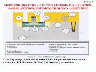
2009 FEP Sub-TWGs and Chairs NEW STRUCTURE FOR FEP CHAPTER in 2009 DEVICE METRICS • Logic Devices [HP, LOP, LSTP]: Prashant Majhi (US) • DRAM Devices: Deoksin Kil (KR) • Flash Devices: Mauro Alessandri (EU) • PCM Devices: Mauro Alessandri (EU) • FeRAM Devices: Yoshimasa Horii (JP) PROCESS METRICS • Starting Materials: Mike Walden (US), Mike Goldstein (US) • Surface Preparation: Joel Barnett (US) • Thermal/Thin Films/Doping: Prashant Majhi (US) • Etch: Tom Lii (US) • CMP: Darryl Peters (US)
FEP 2009 Participants Danel Adrien, Mauro Alessandri, Luis Aparicio, Sehgal Aksey, Amulya Athayde, Souvik Banerjee, Joel Barnett, Twan Bearda, Meridith Beebe, Steve Benner, Ivan (Skip) Berry, Chris Borst, William Bowers, Ian Brown, Arifin Budihardio, Murray Bullis, Mayank T. Bulsara, Jeff Butterbaugh, George K. Celler, Cetin Cetinkaya, Luke Chang, Victor Chia, Phil Clark, Lee Cook, Jeffrey Cross, Suman Datta, Carlos H. Diaz, Roxanne Dulas, Paul Feeney, Graham Fisher, Nich Fuller, Mike Fury, Glenn Gale, Yehiel Gotkis, Mike Goldstein, Christina Gottschalk, Aomar Halimaoui, Qingyuan Han, Dick Hockett, Andrew Hoff, Yoshimasa Horii, Greg Hughes, William Hughes, Raj Jammy, Ravi Kanjolia, Bruce Kellerman, Deoksin Kil, Hyungsup Kim, Simon Kirk, Brian Kirkpatrick, Hiroshi Kitajima, Martin Knotter, Daniel Koos, Larry Larson, Jeff Lauerhaas, Yannick Le Tiec, Kun Tack Lee, Jooh Yun Lee, Tom Lii, Hong Lin, Prashant Majhi, Tom McKenna, Paul Mertens, Katsuhiko Miki, Ichiro Mizushima, Mansour Monipour, Paul Morgan, Brian Murphy, Anthony Muscat, Sadao Nakajima, Yasuo Nara, Masaaki Niwa, Toshihide Ohgata, Hiroshi Oji, Jin Goo Park, Friedrich Passek, Eric Persson, Darryl Peters, Gerd Pfeiffer, Jagdish Prasad, Rick Reidy, Karen Reinhardt, Hwa sung Rhee, Rob Rhoades, Marcello Riva, Jae Sung Roh, Akira Sakai, Archita Sengupta, YugYun Shin, James Shen, Wolfgang Sievert, Chris Sparks, Robert Standley, Sing Pin Tay, Bob Turkot, Steven Verhaverbeke, Hitoshi Wakabayashi, Mike Walden, Masaharu Watanabe, Han Xu
HP Logic Devices • New Table Structure • Individual tables to focus on device metrics for HP, LOP, and LSTP • New scaling approach coordinated with PIDS • reset CV/I benchmark in 2009 to 0.82 ps • CV/I improvement factor changed to 13% per year • New Model Assumptions and New Rows; Parasitic Resistance Constraint • Id, sat not matched to PIDS table Plan to resolve in 2010
LSTP Logic Devices • New scaling approach coordinated with PIDS • reset CV/I benchmark in 2009 [CV/I improvement factor changed to 13% per year] • include Poly/SiON gate stacks through 2010, possibly extended to 2013
Timing of CMOS Innovations LOP bulk CMOS LSTP bulk CMOS 2009 2010 2011 2012 2013 2014 2015 2016 2017 2018 2019 2020 2021 HP bulk CMOS HP UTB/FDSOI HP Multi-Gate LOP UTB/FDSOI LOP Multi-Gate LSTP UTB/FDSOI LSTP Multi-Gate
DRAM • ORTC/PIDS a factor drops from 6 to 4 in 2011 this was not captured in 2009 FEP DRAM Table and will be corrected in 2010 update • capacitance per cell reduced from 25 to 20 pF in 2012 due to expected introduction of buried word line • capacitor dielectric constant reduced and no longer peaks at 130 • capacitor dielectric constant physical thickness reduced no longer red • A/R yellow in 2011 and red in 2013
Potential Dielectric Thickness Problem 2009 ITRS DRAM Roadmap Physical thickness increases as the permittivity increases maintaining a certain leakage current enough room?
Flash • Floating Gate Flash: need for transition to high-k interpoly dielectric moved to 25 nm for NAND and other minor adjustments • New Table added for planar Charge-Trapping Flash that includes: • Tunnel dielectric: EOT thickness, Material/structure to be used, Max leakage current (for retention purpose) measured @ highest write/erase voltage, Erase/program time degradation at constant voltage • Charge Trapping layer: Minimum trap density, Trap energy level, Minimum band offset vs conduction band of the tunnel dielectric and the blocking dielectric (eV), Dielectric constant, Material/structure to be used • Blocking Dielectric: EOT thickness, Max leakage current (for retention purpose) measured @ highest write/erase voltage, Material/structure to be used • Gate: Working function, Material/structure to be used
PCRAM • Added conformality of the PCM cell sealing dielectric. • The challenge in this case is to achieve conformality within a very low thermal budget compatible with the phase change material
FeRAM • Table parameters, general trend are unchanged • Trends in 4-year blocks
FeRAM - forward to high density memory - High-Density and High Speed 128Mb Chain FeRAM with SDRAM- Compatible DDR Interface Shimojo et al. (Toshiba, VLSI technology symposium 2009) High-density cover film and low-damage ferroelectric capacitor etching technique realize 128Mb FeRAM.
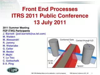
Starting Materials • Alignment of 450mm substrate timing with ISMI projections • New ORTC and related chip size / gate length models have been utilized • Pull-in of 45nm particle size from 2012 to 2010 • Defect densities no longer allowed to increase from the previous generations’ values based upon industry realities • Near-term improvement in SOI BOX and layer thickness capabilities noted – Partially depleted SOI removed from table beginning with 15nm MPU technology generation • Colorization updated
Surface Preparation • Particle metrics updated for changes in DRAM models • Current particle metrology is a challenge at “Critical Particle Diameter” • Material loss metrics colorization removed for DRAM • Achieving material loss goals for advanced logic remains a challenge
Thermal/Thin Films/Doping • Emphasis on Scaled Junctions (to allow for Lg scaling) and External Resistance (scaled contact Rco)
Etch • New Methodology to address gate length variation • contributions from lithography and etch cannot be treated separately • advanced process control allows lithography tools to make field-to-field adjustments to account for both lithography and etch variations across the wafer • Etch inputs coordinated between FEP and LITHO • Physical gate length variation include several random variations listed in table below
CMP • Shallow Trench Isolation CMP requirements table New in 2009 • CMP inputs coordinated between FEP and Interconnect TWGs • Scaled from 130nm Equipment Performance Metrics (EPM) • Real data from end users is difficult to obtain • Broadly applicable, accurate models are not available • Scaled EPMs will be used for baseline CMP metrics going forward, to be refined by data when available • Defectivity, especially microscratches, are a challenge • Significant yield impact and reliability issue • Improvements needed in WIW and WTW uniformity • Post-CMP cleans are not addressed in ITRS • Cleans can have an impact on metal gate work function
FEP Difficult Challenges≥ 16 nm (Metal 1 1/2-pitch) • Strain Engineering- continued improvement for increasing device performance - application to FDSOI and Multi-gate technologies • Achieving DRAM cell capacitance with dimensional scaling- finding robust dielectric with dielectric constant of ~60 - finding electrode material with high work function • Achieving clean surfaces free of killer defects- with no pattern damage - with low material loss (<0.2 A) • High-k/Metal Gate- introduction to full scale manufacturing for HP, LOP, and LSTP - scaling equivalent oxide thickness (EOT) below 0.8nm • 450mm wafers - meeting production level quality and quantity
FEP Difficult Challenges< 16 nm (Metal 1 1/2-pitch) • Continued scaling of HP multigate device in all aspects: EOT, junctions, mobility enhancement, new channel materials, parasitic series resistance, contact silicidation. • Lowering required DRAM capacitance by 4F2 cell scheme or like, while continuing to address materials challenges • Continued achievement of clean surfaces while eliminating material loss and surface damage and sub-critical dimension particle defects • Continued EOT scaling below 0.7 nm with appropriate metal gates • Continued charge retention with dimensional scaling and introduction of new non-charged based NVM technologies
2009 FEP - Highlights • Logic Devices: • Separate tables for HP, LOP, LSTP; CV/I reset with 13% pace; HP Ioff set at 100nA/um • Incorporated new Lg pacing • DRAM Devices: • Node capacitance adjusted for buried wordline; Capacitor dielectric requirement eased/smoothed • Non-volatile memories • Flash – New Charge Trapping Flash Table added • PCRAM – Conformality of Sealing Dielectric added • FeRAM – minor changes; pacing captured in 4-year blocks • Starting Materials: • Incorporated new ORTC scaling and recalculated allowable defects • Near-term improvement in SOI BOX and layer thickness capabilities noted (color changed) • Surface Preparation: • Incorporated new ORTC scaling and recalculated allowable defects • Metrology not capable of monitoring killer defect size • Thermal/Thin Films/Doping: • New table which is split from previous logic device tables • Emphasis on Scaled Junctions and External Resistance • Etch: • New methodology for tracking gate length variation requirements accounting for currently used Advanced Process Control capabilities in lithography. • CMP: • New table for 2009; scratches and uniformity requirements are projected