ITRS 2003 Front End Processing Challenges
ITRS 2003 Front End Processing Challenges. *Gate Stack Leff Control *Memory Cells Dopant Control Contacts *Starting Material FEP Grand Challenge – Material Limited Scaling. David J. Mountain. Why are materials a grand challenge?. MOSFET material development

ITRS 2003 Front End Processing Challenges
E N D
Presentation Transcript
ITRS 2003Front End Processing Challenges *Gate Stack Leff Control *Memory Cells Dopant Control Contacts *Starting Material FEP Grand Challenge – Material Limited Scaling David J. Mountain
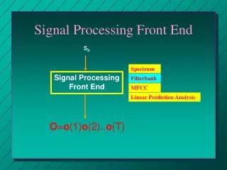
Why are materials a grand challenge? MOSFET material development 1965 (Moore’s Law) – MOS is really Aluminum/SiO2/Silicon Materials: Aluminum, SiO2, Silicon, Boron, Phosphorous 1985 (CMOS) – MOS is really Polysilicon/SiO2/Silicon New materials: Arsenic, Refractory Metals (Ti, Ta, W), Nitride 2005 (Today) – MOS is really Polycide/Nitrided SiO2/Modified Silicon New materials: Copper, Germanium 2015 (End of Moore’s Law?) – MOS will be ??/??/Modified silicon New materials: metal gate, gate dielectric, nickel silicide, others??
MOSFET device structure 1965 Leff ~20 microns: Al gate, SiO2 dielectric and isolation 1985 Leff ~1.25 microns Self-aligned and silicided Source/Drain Polysilicon gate with silicide LOCOS isolation 2005 Leff ~0.032 microns Oxynitride gate dielectric Strained Silicon (Ge implants) Lightly-doped source/drain extensions with nitride spacer 2015 Leff ~0.01 microns FinFET structure Metal gates, unknown material – multi-gate designs Unknown high-k gate dielectric Elevated Source/Drain Strained SOI starting material
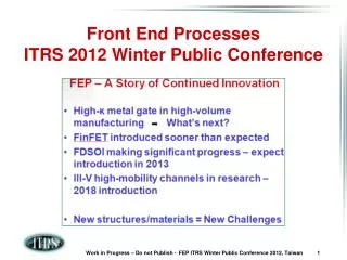
Looking ahead “... solution to a large number of process integration issues arising from a fully 3-D transistor design must be dealt with before the successful introduction of multi-gate, fully depleted CMOS production. These challenges, added to the anticipated shifts to high-K gate dielectrics and dual-workfunction, metal-gate materials, constitute a revolutionary change in transistor technology in the coming 5-7 years.” Why is this revolutionary change? We are adding new materials faster than ever ... to the most critical part of the transistor for the first time ... while the basic device structure is being substantially modified
Gate Stack Need high-K material to replace SiO2 because direct tunneling caused gate leakage current to explode at 1.5 nm thickness Roadmap requires a dielectric with equivalent oxide thickness (EOT) of <1 nm by 2006-2007 with High quality interface to silicon Low leakage Compatibility with subsequent processing steps Long-term reliability Status – Likely candidates have been identified (HfO2 or ZrO2) Need substitute(s) for poly gate due to depletion layer effects Roadmap requires this in 2007-2008 time frame Status – Some materials (Ta, Ru, Pt) are being examined Historical perspective – it took ~10 years to go from demonstrating basic copper processing to use of copper in production (1988-1998)
Memory Cells Stacked capacitor DRAM Change from Metal-Insulator-Silicon (MIS) to Metal-Insulator-Metal (MIM) structure in 2007 Increase k-value from 22 (today) to 60 (2012) to 100 (2018) Trench Capacitor DRAM Change from Silicon-Insulator-Silicon (SIS) to MIS (2007) to MIM (2010) High-k introduction can lag behind stacked capacitor roadmap Process integration issues may be very difficult due to potential limitations in temperature when introducing metal electrodes Ferroelectric RAMs (FeRAMs) are a relatively recent addition (2001 ITRS) to the roadmap; much materials work needs to be done
Starting Substrate Ongoing evolution of mobility enhancements (strained silicon, dual strained silicon, etc.) is expected to continue SOI will see increased use due to reduced parasitic capacitance and ease of introducing multiple gate FETs and other non-planar structures and architectures Introduction of >300 mm wafers (presumably 450 mm) is needed by 2011, but equipment development costs are a major issue 675 mm wafer size is projected in ~2020 if wafering techniques can be scaled that far