Silicon Detector “ Basics ”
Silicon Detector “ Basics ”. The Rise and Rise of silicon in HEP Why silicon? Basic principles & performance More exotic structures; double sided, double metal, pixels… Radiation Damage Real Life Quality Control & Large Systems Testbeams: what can you expect? Operational experience.


Silicon Detector “ Basics ”
E N D
Presentation Transcript
Silicon Detector “Basics” • The Rise and Rise of silicon in HEP • Why silicon? • Basic principles & performance • More exotic structures; double sided, double metal, pixels… • Radiation Damage • Real Life • Quality Control & Large Systems • Testbeams: what can you expect? • Operational experience March 27th 2012 Paula Collins, CERN
Silicon Trends Basic idea amplifier • Start with high resistivity silicon • More elaborate ideas: • n+ side strips – 2d readout • Integrate routing lines on detector • Floating strips for precision • make radiation hard Al strip p+ + + SiO2/Si3N4 - - + n bulk + n+ - + Vbias Hybrid Pixel sensors Chip (low resistivity silicon) bump bonded to sensor Floating pixels for precision chip chip n+ p chip n+ DEPFET: Fully depleted sensor with integrated preamp chip 3d integration techniques MAPS: standard CMOS wafer Integrates all functions CCD: charge collected in thin layer and transferred through silicon
The LEP era Singapore Conference, 1990 ‘The LEP experiments are beginning to reconstruct B mesons… It will be interesting to see whether they will be able to use these events’ Gittleman, Heavy Flavour Review 10 fun packed years later, heavy flavour physics represented 40% of LEP publications
What did Vertex Detectors do? Reconstruct Vertices Flavour tagging Some help in tracking Even some dE/dx!
s = r2s1 + r1s2 (r2 – r1)2 Vertex Detector Performance Dependent on geometry We want: r1 small, r2 large, s1,s2 small Hence the drive at LEP and SLD to decrease the radius of the beampipe and add more layers SLD
2 s2 = A2 + B p sin3/2q Vertex Detector performance And on multiple scattering where A comes from geometry and resolution and B from geometry and MS impact parameter precision On DELPHI, A=20 and B=65 mm momentum • Hence the drive at LEP/SLD for • Beryllium beampipe • Double sided detectors • super slim CCD’s • etc. b physics is here!
LEP vertex detector timeline 1989, ALEPH & DELPHI install prototype modules 1990, ALEPH & DELPHI install first complete barrels ALEPH read rz coordinate with “double sided” detectors 1991, all Beampipes go from Al with r=8 cm to r=5.3 cm Be DELPHI installs three layer vertex detector OPAL construct and install detector in record speed 1992, L3 2 layer double sided vertex detector 1993, OPAL install rz readout with back to back detectors 1994, DELPHI double sided detectors and “double metal” readout 1996, DELPHI install “LEP II Si Tracker” with mstrips, ministrips & pixels
Impact on t physics A delicate measurement! 3 prong vertices
Impact on t physics Dawn of LEP… NB prediction also moved due to mt – non LEP
Impact on b physics • e.g. lifetimes: • Early measurements relied on • inclusive impact parameter methods • B Jy X • Also, a rich programme • - lifetime heirarchy • Bs observation • spectroscopy • baryons • Z0 couplings • mixing • QCD • CKM • etc. etc. with, at first, some odd results
The LHC Era: High Rates, High Multiplicity at full luminosity L=1034 cm-2 s-1: • ~23 overlapping interactions in each bunch crossing every 25 ns ( = 40 MHz ) • inside tracker acceptance (|h|<2.5) 750 charged tracks per bunch crossing • per year: ~5x10¹⁴ bb; ~1014tt; ~20,000 higgs; but also ~1016 inelastic collisions • severe radiation damage to detectors • detector requirements: speed, granularity, radiation hardness a H->bb event a H->bb event as observed at high luminosity plus 22 minimum biasinteractions
Large Systems DELPHI 1990 DELPHI 1994 DELPHI 1996 CMS 2007 2 ! CDF 2001
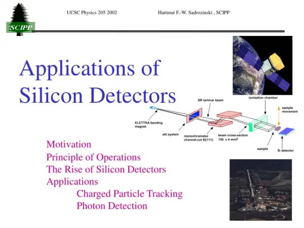
Why Use Silicon? • First and foremost: Spatial resolution • Closely followed by cost and reliability high rates and triggering Traditional Gas Detector 50-100 mm Yes No Emulsion 1 mm Yes Silicon Strips 5 mm • This gives vertexing, which gives lifetimes , quark identification mixing background suppression B tagging …… and a lot of great physics!
Basic Principles • A solid state detector is an ionisation chamber Sensitive volume with electric field • Energy deposited creates e-h pairs • Charge drifts under E field • Get integrated by ROC • Then digitized • And finally is read out and stored
Material PropertiesSemiconductors and Energy bands • Silicon is a group IV semiconductor. Each atom shares 4 valence electrons with its four closest neighbours through covalent bonds • The intrinsic carrier concentration ni is proportional to • where Eg, the band gap energy is about 1.1 eV and kT=1/40 eV at room temperature • At low temperature all electrons are bound and the conduction band is empty • At higher temperature thermal vibrations break some of the bonds, causing some electrons to jump the gap to the conduction band • The remaining open bonds attract other e- and the holes change position (hole conduction) • In pure silicon the intrinsic carrier concentration is 1.45x1010 cm-3 and about 1 in 1012 silicon atoms are ionised
Material PropertiesMobility, Resistivity, and ionisation energy Drift Velocity of charge carriers: Mobility of the charge carriers depends on the mean free time between collisions electron mobility > hole mobility Eventually, the drift velocity saturates. Values of up to 107 cm/s for Si at room temperature are reasonable Resistivity of the silicon depends on The electron and hole mobility The densities of electrons (n) and holes (p) (for doped material one type will dominate) Typical values are 300 kWcm for pure silicon and 5-30 kWcm for doped samples, depending on requirement Ionization energy is the energy loss required to ionise an atom. For silicon this is 3.6 eV, with the rest of the energy going to phonon excitations. For a charged particle, typical energy loss is 3.9 MeV/cm C.A. Klein, J. Applied Physics 39 (1968) 2029
Constructing a detectorSimple calculation of currents in silicon detector • Thickness : 0.03 cm • Area: 1 cm2 • Resistivity: 300 kWcm • Resistance (rd/A) : 9 kW • Mobility (electrons) : 1400 cm2/Vs • Collection time: ~ 10 ns • This needs a field of E=v/m = 0.03 cm/10ns/1400cm2/Vs ~ 2100 V/cm or V=60V • Charge released : ~ 25000 e- ~ 4 fC What currents can we expect? Signal current: Is = 4 fC/10 ns = 400 nA Background current: IR = V/R ~ 60V/9000W ~ 7 mA Alternative way of viewing the same problem: Number of signal e-h+ pairs: 25000 Number of background e-h+ pairs: 1.4 x 1010 x 0.03cm x 1 cm2 = 4 x 10⁸ 0.03cm Background is four orders of magnitude higher than signal!!
Creating a pn junctionDoped materials Doping is the replacement of a small number of atoms in the lattice by atoms of neighboring columns from the atomic table (with one valence electron more or less compared to the basic material). The extra electron or hole is loosely bound. Typical doping concentrations for “high resistivity” Si detectors are 1012 atoms/cm3 for the bulk material In an “n” type semiconductor, electron carriers are obtained by adding atoms with 5 valence electrons: arsenic, antimony, phosphorus. Negatively charged electrons are the majority carriers and the space charge is positive. The fermi level moves up. In a “p” type semiconductor, hole carriers are obtained by adding atoms with 3 valence electrons: Boron, Aluminimum, Gallium. Positively charged “holes” are the majority carriers and the space charge is negative. The fermi level moves down.
Creating a pn junctionDoped materials When brought together to form a junction, the majority diffuse carriers across the junction. The migration leaves a region of net charge of opposite sign on each side, called the space-charge region or depletion region. The electric field set up in the region prevents further migration of carriers. – – + – – – + + + + + + – + + – – + + + + + – Dopant concentration Space charge density Carrier density Electric field Electric potential
Creating a pn junctionReverse Bias Operation The depleted part is very nice, but very small. Apply a reverse bias to extend it, putting the cathode to p and the anode to n. This pulls electrons and holes out of the depletion zone, enlarges it, and increases the potential barrier across the junction. The current across the junction is very small “leakage current” Now, electron-hole pairs created by the traversing particles dominate., and can drift in the electric field That’s how we operate the silicon detector!
Properties of the depletion zone (1) Depletion width is a function of the bulk resistivity, charge carrier mobility m and the magnitude of the reverse bias voltage Vb. If Nd>>NA then – Depleted zone w Vb d + undepleted zone The voltage needed to completely deplete a device of thickness d is called the depletion voltage, Vd. • Need a higher voltage to fully deplete a low resistivity material. • The carrier mobility of holes is lower than for electrons Thickness : 0.03 cm Nd = 1012 cm-3 Silicon permitivity: 11.7 x 8.8 x 10-14 = 1 x 10-12 cm-1 q = 1.6 e-19 Mobility (electrons) : 1400 cm2/Vs Resistivity: 1./(q x m x Nd) = 4.5 kWcm Vd= 50V
Properties of the depletion zone (2) • The capacitance is simply the parallel plate capacity of the depletion zone. One normally measures the depletion behaviour (finds the depletion voltage) by measuring the capacitance versus reverse bias voltage. C = A sqrt ( / 2Vb ) capacitance vs voltage 1/C2 vs voltage Vd
Routinely used LHCb VELO Production Database
The p-n junctionCurrent-Voltage Characteristics The actual current drawn under reverse bias is very important for routine operation. It is dominated by thermally generated e-h+ pairs and has a exponential temperature dependence Typical current-voltage of a p-n junction (diode): exponential current increase in forward bias, small saturation in reverse bias Room temperature leakage current measurement from CMS strip detector
Position Reconstruction So far we described pad diodes. By segmenting the implant we can reconstruct the position of the traversing particle in one dimension p side implants + x + - Typical values used are pitch : 20 mm – 200 mm bulk thickness: 150 mm – 500 mm - + -
Position ReconstructionDC and AC coupled strips • Strips: heavily implanted boron • Substrate: Phosphorus doped (~2-10 kWcm and ~ 300 mm thick; Vfd < 200V) • Backside Phosphorus implanct to establish ohmic contact • High field region close to electrodes • Bias resistor and coupling capacitance integrated directly on sensor • Capacitor as single or double SiO2/Si3N4 layer ~ 100 nm thick • Long snakes of poly resistors with R>1MW
Protecting the edges Slide taken from T. Rohe
Signal size I Ionising energy loss is governed by the Bethe-Bloch equation We care about high energy, minimum ionising particles, where dE/dx ~ 39 KeV/100 mm An energy deposition of 3.6 eV will produce one e-h pair So in 300 mm we should get a mean of 32k e-h pairs Data-Theory comparison Fluctuations give the famous “Landau distribution” The “most probable value” is 0.7 of the peak For 300 mm of silicon, most probable value is ~23400 electron-hole pairs Nucl. Instr. and Meth. A, Vol 661, Issue 1, January 2012, Pages 31-49
noise distribution Landau distribution with noise Noise I Noise is a big issue for silicon detectors. At 22000e- for a 300 mm thick sensor the signal is relatively small. Signal losses can easily occur depending on electronics, stray capacitances, coupling capacitor, frequency etc. If you place your cut too high you cut into the low energy tail of the Landau and you lose efficiency. But if you place your cut too low you pick up fake noise hits Performance of detector often characterised as its S/N ratio
Noise II Usually expressed as equivalent noise charge (ENC) in units of electron charge e. (Here we assume the use of most commonly used CR-RC amplifier shaper circuit) • Main sources: • Capacitive load (Cd ). Often the major source, the dependence is a function of amplifier design. Feedback mechanism of most amplifiers makes the amplifier internal noise dependent on input capacitive load. ENC Cd • Sensor leakage current (shot noise). ENC √ I • Parallel resistance of bias resistor (thermal noise). ENC √( kT/R) • Total noise generally expressed in the form (absorbing the last two sources into the constant term a): ENC = a + b·Cd • Noise is also very frequency dependent, thus dependent on read-out method • Implications for detector design: • Strip length, device quality, choice of bias method will affect noise. • Temperature is important for both leakage current noise (current doubles for T≈7˚C) and for bias resistor component
Noise IV • Some typical values for LEP silicon strip modules (OPAL): • ENC = 500 + 15 ·Cd • Typical strip capacitance is about 1.5 pF/cm, strip length of 18cm so Cd=27pF so ENC = 900e. S/N ≈ 25/1 • Some typical values for LHC silicon strip modules • ENC = 425 + 64 ·Cd • Typical strip capacitance is about 1.2pF/cm, strip length of 12cm so Cd=14pF so ENC = 1300e S/N ≈ 17/1 Capacitive term is much worse for LHC in large part due to very fast shaping time needed (bunch crossing of 25ns vs 22s for LEP)
Signal Diffusion = 2Dtd , where D is the diffusion constant, D=kT/q • Diffusion is caused by random thermal motion • Size of charge cloud after a time td given by • Charges drift in electric field E with velocity v = E m • m = mobility cm2/volt sec, depends on temp + impurities + E: typically 1350 for electrons, 450 for holes • So drift times for: d=300 mm, E=2.5Kv/cm: td(e) = 9 ns, td(h)=27 ns • For electrons and holes diffusion is roughly the same! Typical value: 8 mm for 300 mm drift. Can be exploited to improve position resolution
pitch s = 12 Position Resolution I Resolution is the spread of the reconstructed position minus the true position For one strip clusters “top hat” residuals For two strip clusters “gaussian” residuals pitch s ≈ 1.5 * (S/N)
Position Resolution II • In real life, position resolution is degraded by many factors • relationship of strip pitch and diffusion width (typically 25-150 mm and 5-10 mm) • Statistical fluctuations on the energy deposition Typical real life values for a 300mm thick sensor with S/N=20 Here charge sharing dominates Here single strips dominate Resolution (mm) Pitch (mm)
Position Resolution III There is also a strong dependence on the track incidence angle At small angles you win At large angles you lose (but a good clustering algorithm can help) Optimum is at tan -1 pitch width
Position Resolution IV Fine pitch is good… but there is a price to pay! $$$$$ The floating strip solution can help • The charge is shared to the neighboring strips via capacitative coupling. We don’t have to read out every strip but we still get great resolution • This was a very popular solution. ALEPH for instance obtained s≈ 12 mm using a readout pitch of 100 mm and an implant pitch of 25 mm • But you can’t have everything for nothing! You can lose charge from the floating strips to the backplane, so you must start with a good signal to noise
Hybrid Pixels (stolen from Hartmann/Krammer/Trischuk..)
Intelligent Pixels Timepix design requestedand funded by EUDET collaboration Conventional Medipix2 counting mode remains. sensor Threshold Addition of a clock up to 100MHz allows two new modes. Time over Threshold Time of Arrival Threshold Analogue amplification Digital processing Pixels can be individually programmed into one of these three modes Time of Arrival counts to the end of the Shutter Time Over Threshold counts to the falling edge of the pulse Chip read-out
Or As Results… Time of Arrival Strontium Source Time over Threshold Ion Beams at HIMAC Charge deposition studies with various Isotopes Space Dosimetry Courtesy L. Pinsky, Univ. Houston
Irradiation • Change of depletion voltage • Due to defect levels that are charged in the depleted region -> time and temperature dependent, and very problematic! • Increase of leakage current • Bulk current due to generation/recombination levels • Damage induced trapping centers • Decrease in collected signal charge