Download
1 / 40
520 likes | 2.87k Views
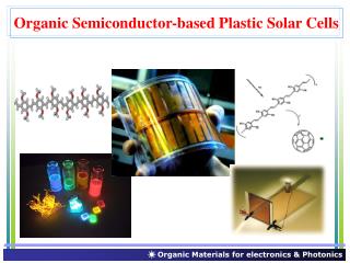
Silicon Nanowire based Solar Cells. ICORE - 2010, Pragya Singh, Pratul K Singh. Outline:Light Trapping in CellsSolar CellEnergy Conversion in Solar CellSolar Cells EverywherePlanar Silicon Solar CellNanowires- PropertiesSilicon Nanowires- PropertiesFabricationTechniques for SiNW DepositionExperiment at the SSN Research Centre.

E N D
1. Silicon Nanowire based Solar Cells International Congress On Renewable Energy
ICORE 2010
2nd December, 2010.
Pragya Singh
Pratul K Singh
2. ICORE - 2010, Pragya Singh, Pratul K Singh
3. Silicon Nanowire based Solar Cells ICORE - 2010, Pragya Singh, Pratul K Singh
4. ICORE - 2010, Pragya Singh, Pratul K Singh
5. ICORE - 2010, Pragya Singh, Pratul K Singh
6. Silicon Nanowire based Solar Cells ICORE - 2010, Pragya Singh, Pratul K Singh
7. Solar Cell Cell is thin Si wafer
Size 10x10 cm : size of a CD
Thickness is in fractions of mm
Metal pattern is to make electrical contacts.
ICORE - 2010, Pragya Singh, Pratul K Singh
8. Silicon Nanowire based Solar Cells ICORE - 2010, Pragya Singh, Pratul K Singh
9. Energy Conversion in Solar Cell Light is shone
Electrons are knocked out
Electrons and holes move in opposite directions
Electrical output is generated between the contacts.
ICORE - 2010, Pragya Singh, Pratul K Singh
10. Silicon Nanowire based Solar Cells ICORE - 2010, Pragya Singh, Pratul K Singh
11. Solar Cells Everywhere �Solar cells :
Safe
Clean
Quiet
Durable
Reliable
Installable anywhere
ICORE - 2010, Pragya Singh, Pratul K Singh
12. The Main Catch ICORE - 2010, Pragya Singh, Pratul K Singh
13. Silicon Nanowire based Solar Cells ICORE - 2010, Pragya Singh, Pratul K Singh
14. ICORE - 2010, Pragya Singh, Pratul K Singh
15. Sliced into Nano-scale ICORE - 2010, Pragya Singh, Pratul K Singh
16. ICORE - 2010, Pragya Singh, Pratul K Singh
17. ICORE - 2010, Pragya Singh, Pratul K Singh
18. Silicon Nanowire based Solar Cells ICORE - 2010, Pragya Singh, Pratul K Singh
19. No Lattice Mismatch.
Flexibility to create heterostructures.
Broad range of materials.
Integration of compound semiconductor based optoelectronic devices with silicon based microelectronics. ICORE - 2010, Pragya Singh, Pratul K Singh Nanowires- Properties
20. Silicon Nanowire based Solar Cells ICORE - 2010, Pragya Singh, Pratul K Singh
21. Recombination:
Poor efficiency may be due to recombination within the bulk silicon element.
Photon strikes the p-n junction in bulk silicon, Produces an electron-hole pair.
Electron and hole must travel along the wire to produce current. ICORE - 2010, Pragya Singh, Pratul K Singh Silicon Nanowires- Properties
22. Recombination:
Tendency to recombine with other oppositely charged charge carrier
Resulting in heat generation rather than electrical energy
ICORE - 2010, Pragya Singh, Pratul K Singh
23. Reduced Recombination in SiNW:
Small diameters.
SiNWs grown vertical, perpendicular to the surface of the substrate.
Electrons strikes on the surface.
Distance of hole/electron travel is minimized.
Distance is of the order of nanometers. ICORE - 2010, Pragya Singh, Pratul K Singh
24. Light Trapping:
Light falling on the substrate gets reflected and once again gets absorbed by silicon nanowires. ICORE - 2010, Pragya Singh, Pratul K Singh
25. Increased Surface Area:
Very narrow pointed structures.
Diameter in nanometers.
Length in micrometers.
Greater area made of p-n junctions is exposed to sunlight.
Increases absorptivity. ICORE - 2010, Pragya Singh, Pratul K Singh
26. ICORE - 2010, Pragya Singh, Pratul K Singh Silicon Nanowires- Properties
27.
Tiny PV Cells:
Composed of 3 layers:
Inner P region
Intrinsic or pure silicon
Outer N region
ICORE - 2010, Pragya Singh, Pratul K Singh
28. Photon strikes the outer shell
Electron-hole pair is created
Travels in the radial direction towards the P layer (core) before recombination. ICORE - 2010, Pragya Singh, Pratul K Singh
29. Silicon Nanowire based Solar Cells ICORE - 2010, Pragya Singh, Pratul K Singh
30. Fabrication Catalyst Particles :
The catalyst must be inert to the reaction products (during CVD nanowire growth).
Gold
Aluminum
Tin
Indium
Gallium
ICORE - 2010, Pragya Singh, Pratul K Singh
31. Silicon Nanowire based Solar Cells ICORE - 2010, Pragya Singh, Pratul K Singh
32. Techniques for SiNW Deposition Techniques:
Supercritical-Fluid-Based and Solution-Based Growth Techniques
Molecular Beam Epitaxy
Laser Ablation
Silicon Monoxide Evaporation
PECVD
ICORE - 2010, Pragya Singh, Pratul K Singh
33. Silicon Nanowire based Solar Cells ICORE - 2010, Pragya Singh, Pratul K Singh
34. Experiment at the SSN Research Centre ICORE - 2010, Pragya Singh, Pratul K Singh
35. Si-NW Growth Principle ICORE - 2010, Pragya Singh, Pratul K Singh
36. Si-NW Deposition Process Steps ICORE - 2010, Pragya Singh, Pratul K Singh Silicon (4 inch) n-type Substrate Cleaned
Chromium layer of 10.7nm deposited by EBE Method
Gold Layer of 2.6nm deposited by EBE Method
37. SiNW � Deposition Experiment Catalyst Nano Particles:
Gold Film Layer (2.6nm) Deposited on Silicon Substrate by EBE
Heated at 580 degrees to form Nano Particles
Figure1 SEM image of Nano particles of Gold
ICORE - 2010, Pragya Singh, Pratul K Singh
38. SiNW � Deposition Experiment PECVD system.
Temperature : 380 degrees
Pressure in mTorr : 500mT
Time of Deposition : 30 minutes
Gases Used : Silane, Hydrogen and Argon
ICORE - 2010, Pragya Singh, Pratul K Singh
39. Si NW Comparison ICORE - 2010, Pragya Singh, Pratul K Singh
40. Thank You ICORE - 2010, Pragya Singh, Pratul K Singh