Download
1 / 15
150 likes | 390 Views
Section I I ntroduction to Programmable Logic Devices. Logic. Standard Logic. ASIC. CPLDs. Programmable Logic Device Families. Source: Dataquest. Common Resources Configurable Logic Blocks (CLB) Memory Look-Up Table AND-OR planes Simple gates Input / Output Blocks (IOB)

E N D
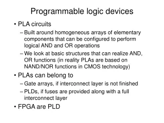
Logic Standard Logic ASIC CPLDs Programmable Logic Device Families Source: Dataquest Common Resources Configurable Logic Blocks (CLB) • Memory Look-Up Table • AND-OR planes • Simple gates Input / Output Blocks (IOB) • Bidirectional, latches, inverters, pullup/pulldowns Interconnect or Routing • Local, internal feedback, and global Programmable Logic Devices (PLDs) Gate Arrays Cell-Based ICs Full Custom ICs SPLDs (PALs) FPGAs Acronyms SPLD = Simple Prog. Logic Device PAL = Prog. Array of Logic CPLD = Complex PLD FPGA = Field Prog. Gate Array
CPLDs and FPGAs CPLD FPGA Complex Programmable Logic Device Field-Programmable Gate Array Architecture PAL/22V10-like Gate array-like More Combinational More Registers + RAM Density Low-to-medium Medium-to-high 0.5-10K logic gates 1K to 500K system gates Performance Predictable timing Application dependent Up to 200 MHz today Up to 135MHz today Interconnect “Crossbar” Incremental Not shown: Simple PLD (SPLD) Architecture
Programmable Logic vs. Semi-Custom ASIC Market Total 1996 Market – $9.5B Total 2001 Market – $15.8B Mask ProgrammedGate Arrays$7.4B Mask ProgrammedGate Arrays$5.6B 47% 59% 20% 21% 37% 16% Standard Logic$2.0B ProgrammableLogic Share $1.9B Standard Logic$2.6B Programmable Logic Share $5.8B Source: Dataquest, May 1997
FPGA Market Share Q4 1997 Source: In-Stat Research, March 1998 Altera number includes both 8K and 10K families
75 50 25 7.5 4Q97 1Q98 2Q98 Process & Density Leadership Virtex 1 Million Gates 0.25u process XC40250XV ~500K gates XC40150XV Transistor Count (millions) XC40125XV - Industry’s 1st 0.25u PLD. ~250K gates, 5 LM. 3Q98 4Q98
Core Class Upper Level Class Research Xilinx Integrated Circuit Products • XC9500: Flash-based In System Program. CPLDs • Lowest price, best pin locking, 600 - 7K gates • XC4000: Industry’s largest & fastest FPGAs • XC4000E: 0.5, 5V, 5K - 40K gates • XC4000EX: 0.5, 5V, 45K - 60K gates • XC4000XL: 0.35, 3.3V devices, 5V compatible I/O, 3K - 180K gates • XC4000XV: 0.25, 2.5V / 3.3V, 5V compatible I/O, 250K - 500K gates • Spartan: 0.5, 5V, Low Cost, 10K - 40K gates • Virtex: New FPGA architecture in 1998 • 0.25, 5LM, 250K-1M gates, Select & Block-RAM • XC6200: Reconfigurable Processing Unit • Dynamically and partially reconfigurable • Low-cost solutions (Industry) • XC3000 (no RAM), XC5200 (no RAM), HardWire X X X X X X X X X X X X X X X * Gates are in terms of system-level gates
3 In-System Programming Controller JTAG Controller JTAG Port Function Block1 I/O I/O Function Block 2 I/O I/O Blocks FastCONNECT Switch Matrix I/O Function Block 3 Global Clocks 3 Global Set/Reset 1 Function Block 4 Global Tri-States 2 or 4 XC9500 CPLDs • 5 volt in-system programmable (ISP) CPLDs • 5 ns pin-to-pin • 36 to 288 macrocells (6400 gates) • Industry’s best pin-locking architecture • 10,000 program/erase cycles • Complete IEEE 1149.1 JTAG capability
Xilinx XC4000 Architecture • High Density -> 1M System Gates • SRAM Based LUT for Synchronous Dual Port RAM or Logic • ASIC-like array structure • Built-in Tri-States • Infinite reconfigurations, downloaded from PC or workstation in ~1 second Configurable Logic Blocks (CLBs) I/O Blocks (IOBs) Programmable Interconnect
XC6200 Reconfigurable Processing Unit 1000x improvement in reconfiguration time from external memory Memory I/O CPU FastMAPtmassures high speed direct access to all internal registers Microprocessor interface built-in: “XC6200 is memory mapped to look like SRAM to a host processor” XC6200 RPU All registers accessed via built-in low-skew FastMAPtm busses High capacity distributed memory permits allocation of chip resources to logic or memory - 256kbits in XC6264 Ultrafast Partial Reconfiguration (40ns to 100’s of usec) I/O Up to 100,000 gates
Logic Cells Logic Gates 1,000,000 12M 1.2M 120K 12K 2 Million logic gates 100,000 10,000 Year 1,000 1994 1996 1998 2000 2002 D Q LUT FF Exponential Growth in Density • Nov. 1997- shipping world’s largest FPGA, XC40125XV (10,982 logic cells, 250K System Gates) • 1 Logic cell = 4-input LUT + FF • 175,000 Logic cells = 2.0 M logic gates in 2001
1 2 M1 Technology XC4000 XC4000 XC4000 Design Flow Design Entry in schematic, ABEL, VHDL, and/or Verilog. Vendors include Synopsys, Aldec (Xilinx Foundation), Mentor, Cadence, Viewlogic, and 35 others. Implementation includes Placement & Routing and bitstream generation using Xilinx’s M1 Technology. Also, analyze timing, view layout, and more. Download directly to the Xilinx hardware device(s) with unlimited reconfigurations* !! 3 *XC9500 has 10,000 write/erase cycles
Foundation Series Delivers Value & Ease of Use • Complete, ready-to-use software solution • Simple, easy-to-use design environment • Easy-to-learn schematic, state-diagram, ABEL, VHDL, & Verilog design • Synopsys • FPGA • Express • Integration*
The Xilinx Student Edition • Prentice Hall’s most requested new engineering product in Q1 ‘98 ! • Complete, affordable, and practical digital design course environment for all students • Predeveloped and tested lab-based course • Includes • Foundation Series 1.3 for students’ computers • Practical Xilinx Designer lab tutorial book • Coupon for XS40-005XL and XS95-108 boards ($129) • Sold through bookstores by Prentice Hall and www.Amazon.com, listed at $79 (ISBN 0136716296) • Integrated tutorial projects cover:TTL, Boolean Logic, State Machines, Memories, Flip Flops, Timing, 4-bit and 8-bit processors • Upgradeable for free to F1.4 Express with VHDL & Verilog, 40K gates, VHDL labs on the web