Programmable Logic Devices
Programmable Logic Devices. General structure of PLDs. Buffer/inverter. ( a ) Symbol ( b ) Logic equivalent. Programming by Blowing Fuses. ( a ) Before programming ( b ) After programming. PLD Notation.


Programmable Logic Devices
E N D
Presentation Transcript
Programmable Logic Devices A. Yaicharoen
General structure of PLDs A. Yaicharoen
Buffer/inverter (a) Symbol (b) Logic equivalent A. Yaicharoen
Programming by Blowing Fuses (a) Before programming (b) After programming A. Yaicharoen
PLD Notation (a) Unprogrammed and-gate (b) Unprogrammed or-gate (c) Programmed and-gate realizing the term ac (d) Programmed or-gate realizing the term a + b (e) Special notation for an and-gate having all its input fuses intact (f) Special notiation for an or-gate having all its input fuses intact (g) And-gate with nonfusible inputs (h) Or-gate with nonfusible inputs A. Yaicharoen
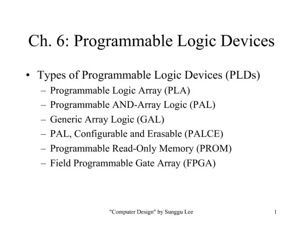
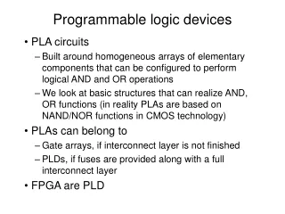
Types of PLDs • Programmable ROM (PROM) • Fixed AND-array, programmable OR-array • Programmable Logic Array (PLA) • Programmable AND-array and OR-array • Programmable Array Logic (PAL) • Programmable AND-array, Fixed OR-array A. Yaicharoen
Structure of a PROM A. Yaicharoen
A 2nm PROM A. Yaicharoen
Using a PROM for logic design A. Yaicharoen
Logic diagram of an n p m PLA A. Yaicharoen
Example Example of combinational logic design using a PLA. (a) Maps showing the multiple-output prime implicants. (b) Partial covering of the f1 and f2 maps. (c) Maps for the multiple-output minimal sum. (d) Realization using a 3 4 2 PLA. A. Yaicharoen
Ex-Or-gate with a Programmable Fuse (a) Circuit diagram. (b) Symbolic representation. A. Yaicharoen
More on PLA General structure of a PLA having true and complemented output capability A. Yaicharoen
Example Karnaugh maps for the functions f1(x,y,z) = m(1,2,3,7) and f2(x,y,z) = m(0,1,2,6) A. Yaicharoen
Example Two realizations of f1(x,y,z) = m(1,2,3,7) and f2(x,y,z) = m(0,1,2,6). (a) Realization based on f1 and 2 (b) Realization based on 1 and 2 A. Yaicharoen
A simple 4-input, 3-output PAL device A. Yaicharoen