Download
1 / 36
370 likes | 539 Views
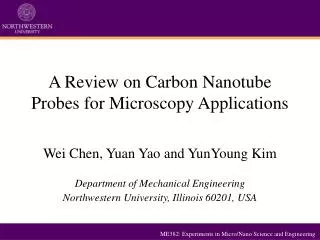
A Review on Carbon Nanotube Probes for Microscopy Applications. Wei Chen, Yuan Yao and YunYoung Kim Department of Mechanical Engineering Northwestern University, Illinois 60201, USA. Contents. Introduction (YunYoung Kim) Gluing Method (Wei Chen) Growng Method (Yuan Yao)

E N D
A Review on Carbon Nanotube Probes for Microscopy Applications Wei Chen, Yuan Yao and YunYoung Kim Department of Mechanical Engineering Northwestern University, Illinois 60201, USA
Contents • Introduction (YunYoung Kim) • Gluing Method (Wei Chen) • Growng Method (Yuan Yao) • Biological Applications (YunYoung Kim)
Introduction Atomic Force Microscopy (AFM) - Indispensable device for micro/nano scale phenomena studies - Surface topology measurement - Micro/nano structure manipulation Carbon Nanotube (CNT) - A new material that has exceptional properties - Promising possibilities of applications (composites, FEP display, chemical sensors, etc.) Hafner et al., Prog. Biophys. Mol. Biol. 77, 73-110 (2001). Hafner et al., Prog. Biophys. Mol. Biol. 77, 73-110 (2001).
CNT Probe Si Tip Si Tip CNT Probe Tang et al., Nano Lett. 5(1), 11-14 (2005). Wong et al., J. Am. Chem. Soc. 120, 603-604 (1998). Introduction CNT-Probed AFM - A CNT (either SWNT or MWNT) is attached on the apex of the conventional silicon AFM cantilever tip.
Guo et al., Appl. Surf. Sci. 228, 53-56 (2004). Chang et al., Jpn. J. Appl. Sci. 43(7B), 4517-4520 (2004). Dai et al., Nature 384(14), 147-150 (1996). Introduction The Synergy Effect of CNT-Probed AFM - Resolution enhancement CNT Probe Si Tip CNT Probe Si Tip - Precise measurements of high aspect ratio structures CNT Probe Si Tip
Introduction - High wear-resistance CNT Probe CNT Probe Si Tip Si Tip Chang et al., Jpn. J. Appl. Phys. 43(7B), 4517-4520 (2004). - Biomolecule manipulation Streptavidin Receptor Biotin Ligand Chang et al., Jpn. J. Appl. Phys. 43(7B), 4517-4520 (2004).
Introduction Overview: Two Ways of CNT-Tip Fabrication - Gluing Method Tang et al., Nano Lett. 5(1), 11-14 (2005). - Growing Method Hafner et al., Prog. Biophys. Mol. Biol. 77, 73-110 (2001).
Gluing Method First trial-”glue” MWNT 5~20nm in diameter 0.25~1μm in length Dai, H. et al. Nature 1996 Pick-up method SWNT 0.9~2.8nm in diameter Lieber et al. J. Phys. Chem. B 2001
Gluing Method Disadvantage • Manual assembly method is time-consuming, needs proficient experimental technique, the fabrication yield is restricted. • Spacial resolution is compromised by the large diameters of attached CNTs, since only thick CNTs can be viewed under optical microscope.
Gluing Method Magnetic field-aligned • Sputter coat the Au film on AFM probes; • Fix the AFM tips; • Prepare and stir CNTs suspension (5mL); • Apply alternative magnetic field (Amplitude B0=0.1T); • CNTs are aligned and attached onto the tips. Average protruding angle: 35o Length: 100-500nm Hall, A. et al. Appl. Phys. Lett. 2003
Change in flux ~ (Induced potential) Induced Current Dipole moments Potential Energy Gluing Method Physical Principle Attraction Force
Gluing Method Dip-Coating & Dielectrophoresis • Introduce the CNTs into the TiO2 SG solution; • W tip was dipped into SG solution containing CNTs; • Apply DC voltage between the tip and the solution; • CNTs was deposited on the tip, and the SG was coated on it as well, • Withdraw the tip and anneal it under infra-red lamp. Diameter: ~9.2nm Length: ~950nm A. Brioude et al. Appl. Surf. Sci. 221 (2004)
Strong adhesion Gluing Method • Many CNTs entangle together into fiber, CNTs break near the apex of tips since the sudden strong current; • The SG thin film works like a sheath, which integrates the CNTs and tip as a whole. Potential for large-scale fabrication A. Brioude et al. Appl. Surf. Sci. 221 (2004)
Growing Method Pore-growth method (first direct growth, Hafner et al., Nature 1999) • Flatten the conventional silicon (Si) tip at its apex by contact AFM imaging; • Anodize the tip in hydrogen fluoride to create nano-pores of 50–100 nm diameter along the tip axis; • Electrodeposit iron catalyst into the nano-pores from FeSO4 solution; • Use Chemical Vapor Deposition (CVD) to grow carbon nanotubes with ethylene and hydrogen at 750℃ for 10 min.
Growing Method 1μm 20nm • The pore-growth method demonstrated the great potential of thermal CVD to grow directly controlled diameter nanotube tips.
Growing Method Limitation: The preparation of a porous layer can be time consuming and may not place individual SWCNTs at the optimal location on the flattened apex.
Growing Method Surface-growth method (Hafner et al., J. Am. Chem. Soc. 1999) • Deposit catalyst onto the pyramidal tip of a commercial cantilever; (Fe-Mo and colloidal Fe-oxide catalysts are electrophoretically deposited on the tip) • grow the SWCNT probe using thermal CVD at 800 ℃ for 3 min. (ethylene is used as carbon source -- C2H4 : H2 : Ar = 1 : 200 : 300)
Growing Method Surface-growth method SEM cannot provide an accurate measure of the tip diameters. TEM analysis was able to demonstrate that the tips consist of individual SWCNT and small SWCNT bundles. 200nm 20nm
Growing Method Surface-growth method Individual SWNT tips can be prepared by lowering the catalyst density on the surface such that only 1 nanotube reaches the apex. Hence, by controlling the catalyst density , it is possible to produce well-defined individual SWNT tips. 10nm
Growing Method Mass production ? Erhan Yenilmez, et al., Appl. Phys. Lett. 2002 How to place catalyst on each of the 375 Si tips on a 4-in wafer ? How to grow SWCNTs on a wafer-scale large substrate using CVD?
Growing Method Catalyst patterning • Spin coat polymethylmethacrylate (PMMA) onto the wafer at a low spin speed of 1000 rpm and bake the wafer on a hot plate at 180 ℃ for 5 min. Repeat the PMMA spin coating and baking step for three times. • Spin coat the catalyst suspension onto the wafer at a low spin speed of 250rpm • Liftoff the PMMA layer in acetone. The catalyst coated around the pyramidal surfaces of the tips will be left.
Growing Method The system is heated to 900 ℃ in an Ar flow after a thorough purge of the system by Ar. Then ultrahigh purity methane (99.999% purity, flow rate of 1500 sccm) is piped through the system together with hydrogen (flow rate of 125 sccm) for a growth time of 7 min. At last, the system is cooled to room temperature in a H2 flow.
Growing Method Their method yields SWCNTs protruding from more than 90% of the 375 Si tips on a wafer.
Growing Method Limitations: • CNT location, density, length, and orientation can not be welled controlled by the thermal CVD methods. • Although we can get many tips through one thermal CVD process, seldom of them has individual free-standing and well-oriented CNTs. The yield of readily usable tips is very low. • After CNT tip fabrication, a one-at-a-time manipulation approach is required to shorten the extruding CNTs for AFM use. • This shortening process decreases the efficiency of mass production. • In addition, nearly all of the previous approaches (including both attaching methods and direct growth methods) rely on commercially available silicon tips or prefabricated commercial silicon probe wafers.
Growing Method Qi Ye et al., Nano Lett. 2004 They integrated nanopatterning and nanomaterials synthesis with traditional silicon cantilever microfabrication technology, and produced 244 CNT probe tips on a 4-in. wafer with controlled CNT location, diameter, length, and orientation.
Growing Method Qi Ye et al., Nano Lett. 2004 PECVD – Plasma Enhanced CVD
Growing Method Qi Ye et al., Nano Lett. 2004 PECVD – Plasma Enhanced CVD
Growing Method Qi Ye et al., Nano Lett. 2004
Growing Method Qi Ye et al., Nano Lett. 2004 Advantages of their approach: • No prefabricated silicon probe wafers needed; • Better control of the CNT location, density, length, and orientation by PECVD; • No need to conduct post-fabrication treatment to remove and/or shorten the CNT tips.
Biological Applications Biomolecule Structure Characterization A staggered end A defect A Y-branch An image of Aβ40 fibril - Amyloid-β fibrils are measured with CNT tips. - The small effective tip radii result in 12~30% increase of resolution. - Observed widths are 3~8 nm smaller for MWNT tips than those for Si tips. Wong et al., J. Am. Chem. Soc.120, 603-604 (1998)
Biological Applications SWNT Tip FWHM=5.6 nm Si Tip FWHM=14.4 nm An image of double-stranded DNA on mica Height cross-section of the DNA - Significant resolution improvement for SWNT tips (full width at half maximum is 5±1 nm for SWNT tip and 15±1 nm for Si tip) - More refined measurements are possible with SWNT tips. Wong et al., Appl. Phys. Lett.73, 3465-3467 (1998)
Biological Applications AFM image of DNA taken using a CNT tip AFM image of DNA taken using a Si tip - Improvement in resolution by a factor of 2 - The diameter ranges from 12 to 15 nm with a Si tip, but 7 to 8 nm with a CNT tip. - Blurred image is observed when the CNT tip with a ~10 nm diameter is longer than 500 nm Nishijima et al., Appl. Phys. Lett74, 4061-4063 (1999)
Biological Applications An Issue about the Length of CNTs - To avoid a mechanical instability, the length should be less than 500 nm for MWNTs and 50nm for SWNTs1. - Akita et al. also reports that L < 500 nm is required for a stable and high-resolution imaging2. Vibration amplitude, a: outer radii of the nanotube (5 nm) b: inner radii of the nanutube (2.5 nm) Y: Young’s modulus (1TPa) - For example, L > 500 nm results in u > 0.5 nm and degradation of resolution by a factor of ten. 1) Chang et al., Jpn, J. Appl. Phys.43, 4517-4520 (2004) 2) S. Akita et al., J. Phys. D.: Appl. Phys.32, 1044-1048 (1999)
A MWNT tip after immersing in DI water A MWNT tip before immersing in DI water Biological Applications Manipulation of Wettability of CNTS - Hydrophobic CNTs are chemically incompatible in aqueous environments. - Stevens et al. reported a failure of MWNT probe during the measurement in DI H2O. Stevens et al., IEEE Trans. Nanobio.3, 56-60 (2004)
Biological Applications - The wettability can be adjusted by depositing ethylendiamine (DE) on the sidewalls of CNTs. - Amine groups can be absorbed onto CNT sidewalls by exchanging of electrons, and render the CNT to be hydrophilic. - The deposition do not change the chemical property of the tip end, and thus do not affect the probe resolution. CNT tip, treated, in air CNT tip, untreated, in air CNT tip, treated, in H2O Si tip, in air Stevens et al., IEEE Trans. Nanobio.3, 56-60 (2004)
Summary 1. CNT-probed AFM is reviewed. 2. CNT-probes can be fabricated by - the gluing method, in which a grown CNT is picked up by a Si tip using adhesives, electric or magnetic fields. - the growing method, in which a CNT is directly grown on the pyramidal surfaces of a silicon tip. 3. Examples of CNT-probe applications for biological studies are presented.