Download
1 / 36
360 likes | 379 Views
Delve into the fundamentals of micro and nanotechnology, from propagation delay to semiconductor energy bands. Learn about logic circuits, gate delays, semiconductor materials, and electronic energy levels. Explore the fascinating world of microdevices and nanotech applications.

E N D
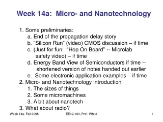
Week 14a: Micro- and Nanotechnology • Some preliminaries: • End of the propagation delay story • “Silicon Run” (video) CMOS discussion – if time • (Just for fun: “Hop On Board” -- Microlab • safety video) – if time • Energy Band View of Semiconductors if time -- • shortened version of notes handed out earlier • e. Some electronic application examples – if time • Micro- and Nanotechnology introduction • The sizes of things • Some micromachines • A bit about nanotech • What about radio? EE42/100, Prof. White
1a. Propagation delay in logic circuits EE42/100, Prof. White
Note becomes valid one gate delay after B switches Note that becomes valid two gate delays after B&C switch, because the invert function takes one delay and the NAND function a second. No change at t =3 tD TIMING DIAGRAMS Show transitions of variables vs time A Logic state B D t C 0 t tD t tD 2tD t tD t 2tD 3tD tD EE42/100, Prof. White
EXAMPLE WHAT IS THE ORIGIN OF GATE DELAY? Logic gates are electronic circuits that process electrical signals Most common signal for logic variable: voltage Specific voltage ranges correspond to “0” or “1” Thus delay in voltage rise or fall (because of delay in charging internal capacitances) will translate to a delay in signal timing Note that the specific voltage range for 0 or 1 depends on “logic family,” and in general decreases with logic generations EE42/100, Prof. White
inside a large system VOLTAGE WAVEFORMS (TIME FUNCTIONS) Inverter input is vIN(t), output is vOUT(t) Vin(t) t EE42/100, Prof. White
Vin(t) 1.5 t Approximation tD tD tD GATE DELAY (PROPAGATION DELAY) Define as the delay required for the output voltage to reach 50% of its final value. In this example we will use 3V logic, so halfway point is 1.5V. Inverters are designed so that the gate delay is symmetrical (rise and fall) Vout(t) 1.5 t EE42/100, Prof. White
WHAT DETERMINES GATE DELAY? 5 MODEL Vx R 2.5 II RC = 0.1ns C 5 vIN vOUT 2.5 Vx t tD = 0.069ns Example The gate delay is simply the charging of the capacitors at internal nodes. Oversimplified example using “ideal inverter, II” and 5V logic swing RC = 0.1ns so 0.069ns after vIN switches by 5V, Vx moves 2.5V EE42/100, Prof. White
VDD = 2V - SP is closed if VIN < VDD SP + RP VOUT VIN + + RN Input Output SN is closed if VIN > VSS + SN - - - VSS = 0V Controlled Switch Model of Inverter So if VIN is 2V then SN is closed and SP is open. Hence VOUT is zero. But if VIN is 0V then SP is closed and SN is open. Hence VOUT is 2V. EE42/100, Prof. White
How fast is this? Speed of light: c = 3 108 m/s Distance traveled in 57 ps is: EFFECT OF PROPAGATION DELAY ON PROCESSOR SPEED Computer architects would like each system clock cycle to have between 20 and 50 gate delays … use 35 for calculations Implication: if clock frequency = 500 MHz clock period = (5108 s1)1 Period = 2 10 9s = 2 ns (nanoseconds) Gate delay must be tD = (1/35) Period = (2 ns)/35 = 57 ps (picoseconds) C X tD = (3x10⁸m/s)(57x10-12) = 17 x 10-4 m = 1.7cm EE42/100, Prof. White
1d. Energy Band View of Semiconductors Conductors, semiconductors, insulators: Why is it that when individual atoms get close together to form a solid – such as copper, silicon, or quartz – they form materials that have a high, variable, or low ability to conduct current? Understand in terms of allowed, empty, and occupiedelectronic energy levels and electronicenergy bands. Fig. 1 shows the calculated allowed energy levels for electrons (vertical axis) versus distance between atoms (horizontal axis) for materials like silicon. EE42/100, Prof. White
Fig. 1. Calculated energy levels in the diamond structure as a function of assumed atomic spacing at T = 0o K. (From “Introduction to Semiconductor Physics”, Wiley, 1964) EE42/100, Prof. White
In Fig. 1, at right atoms are essentially isolated; at left atomic separations are just a few tenths of a nanometer, characteristic of atoms in a silicon crystal. • If we start with N atoms of silicon at the right, which have 14 electrons each, there must be 14N allowed energy levels for the electrons. (You learned about this in physics in connection with the Bohr atom, the Pauli Exclusion principle, etc.) • If the atoms are pushed together to form a solid chunk of silicon, the electrons of neighboring atoms will interact and the allowed energy levels will broaden intoenergy bands. EE42/100, Prof. White
When the “actual spacing” is reached, the quantum-mechanical calculation results are that: • at lowest energies very narrow ranges of energy are allowed for inner electrons (these are core electrons, near the nuclei); • a higher band of 4N allowed states exists that, at 0oK, is filled with 4N electrons; • then an energy gap, EG, appears with no allowed states (no electrons permitted!); and • at highest energies a band of allowed states appears that is entirely empty at 0oK. • Can this crystal conduct electricity? EE42/100, Prof. White
NO, it cannot conductor electricity at 0o K because that involves moving charges and therefore an increase of electron energy – but we have only two bands of states separated by a forbidden energy gap, EG. The (lower) valence band is entirely filled, and the (upper) conduction band states are entirely empty. To conduct electricity we need to have a band that has some filled states (some electrons!) and some empty states that can be occupied by electrons whose energies increase. EE42/100, Prof. White
Metals, pure silicon at 0K and 300K, and doped silicon • A. Conductors such as aluminum and gold can conduct at low • temperatures because the highest energy band is only partly • filled – there are electrons and there are empty states they can • move into when caused to move by an applied electric field. • B. Silicon at 0K – can’t conduct because the highest band containing • electrons is filled. • Pure silicon at room temp. is slightly conductive since thermal • energy can raise some electrons to the mostly empty conduction • band. • Silicon doped with donors (like P or As) can conduct (and • Become n-type) better than pure silicon at room temp. since it doesn’t • take much energy to free a valence electron so it can enter the • conduction band. • Silicon doped with acceptors (like B) can conduct (and become • p-type) at room temp. since it doesn’t take much energy to free a • valence electron and create a hole in the valence band. EE42/100, Prof. White
A. Metal B. Pure Si 0K C. Pure Si at 300K D. n-type Si E. p-type Si Conduction band + + + Forbidden energy band (energy gap) Donor level Acceptor level - - - Valence band EE42/100, Prof. White
2. Micro- and Nanotechnology EE42/100, Prof. White
The Sizes of Things EE42/100, Prof. White
(Gordon) Moore’s Law EE42/100, Prof. White
Inkjet printer head: A thin-film heater behind each nozzle vaporizes the ink and ejects a droplet of ink EE42/100, Prof. White
Micro-guitar from Cornell University (the strings actually vibrate when plucked) EE42/100, Prof. White
Early micromachine (with dead mite) EE42/100, Prof. White
Laser scanning micromachine with electrostatic motors, gears, and mirror EE42/100, Prof. White
Micromachine: Safety lock for nuclear bomb EE42/100, Prof. White
Digital Light Projector (Texas Instruments) EE42/100, Prof. White
16-micron-square tilting mirrors built over CMOS drive circuit EE42/100, Prof. White
Microstructures etched in Teflon -- useful in BioMEMS applications EE42/100, Prof. White
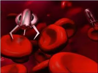
Nanotechnology Defining Dimension: Involves products and processes with significant features 100 nanometers and smaller. (To be listed in Merrill Lynch nanotechnology index, a company must indicate in a public document that nanotechnology initiatives are a significant component of their business strategy) Significant because of unusual properties: Mechanical – very strong; new devices (e.g., motor) Physics – new phenomena (e.g., metallic or semiconducting) Chemical – Reactivity, tiny hollow structures (e.g., can carry drugs into body) EE42/100, Prof. White
Nanotech examples Uses demonstrated: Electrostaically driven nanomotor (Alex Zettl, UCB Physics) Field effect transistors and logic devices (Ph. Avouris, Nano-Letters 16 Aug. 2001) – NOR gate, flip-flop memory cell, ring oscillator) Sensors (Nanometrix Co.) – hydrogen sensing by palladium- coated silicon nanotube operating as an FET Liquid repellent cloth Cautions (research needed): “Gray goo” – if nanotech replicating structures are made they could take over the Earth Nanostructures can pass through/around cells in the body Nanostructures may clump in liquids and have limited uses in environmental remediation, drug delivery EE42/100, Prof. White
C60 -- Buckeyball EE42/100, Prof. White
Nano structures Carbon nanotube field-effect transistor EE42/100, Prof. White
3. What About Radio? EE42/100, Prof. White
Amplitude Modulation (AM) Radio EE42/100, Prof. White
Frequency Modulation (FM) Radio EE42/100, Prof. White
Crystal Set AM Radio Receiver – no batteries! EE42/100, Prof. White