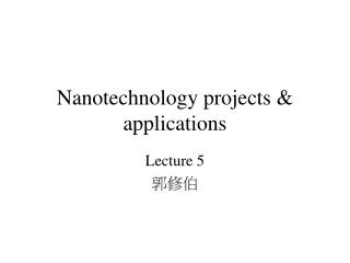
Nanotechnology projects & applications
Nanotechnology projects & applications. Lecture 5 郭修伯. Frontiers of nanotechnology from Asia-Pacific Nanotech Forum. ( Tsukuba, 2002). The vision and strategy of the US national nanotechnology initiative. M.C. Roco US national science foundation. History. 1981

Nanotechnology projects & applications
E N D
Presentation Transcript
Nanotechnology projects & applications Lecture 5 郭修伯
Frontiers of nanotechnology from Asia-Pacific Nanotech Forum (Tsukuba, 2002)
The vision and strategy of the US national nanotechnology initiative M.C. Roco US national science foundation
History • 1981 • able to measure the size of an atom cluster on a surface (IBM, Zurich) • 1991 • able to move atoms on surface (IBM, Almaden) • 2002 • able to assemble the molecules by physically positioning the component atoms
Nanotechnology • National Nanotechnology Initiative (NNI) • Long-term visionary program since 01/2000 • 22 departments and independent agencies • 961 million (2004) • Government investments worldwide ~ 4 billion • international collaborations and competitions
NNI nanotechnology • Definition • Nanotechnology is working - measuring, manipulating and controlling - at the atomic, molecular and supramolecular levels, at a length scale of approximately 1 - 100 nm, in order to understand and create materials, devices, and systems with fundamentally new properties and functions because of their small structures.
Commercialization • 1st generation (commercialized) • passive nanostructure • applied in coatings, nanoparticles, bulk materials (nanostructured metals, polymers and ceramics) • towards systematic design method • 2nd generation • active nanostructure • transistors, amplifier,targeted drugs and chemicals, and adaptive structures (~2005)
Commercialization • 3rd generation • systems of nanosystems • 3D features, heterogeneous nanocomponents • specific assembly techniques (such as bio-assembly, networking at the nanoscale, new architectures) • ~2010 • 4th generation • molecular nanosystems • nanodevices, biomimetics and new molecular designs (~2020)
Nanotechnology for the next generation T.Nakahara & T. Imai Sumitomo Electric Industries Ltd.
Policies • Similar projects from • Nanocarbon materials • nanoelectronics • nanobiomaterials • Others? • Diamond nanoemitter project
Targets • Size!
Small size effect • Compressed ferrous alloy powder • due to resonance: • high electromagnetic wave adsorption in the microwave frequency region • adjust particle shape and metal composition: • different absorption peak from 0.5 ~ 5G Hz • For small and precise communication • mobilephones, PC, etc.
Nano size effect • Nanomaterial: diamond • rigid atomic structure • high hardness, high thermal conductivity and high acoustic velocity • semiconductor properties • apply as semiconductor devices, optical devices, electron emission devices • fabrication and synthesis technology • manufactured very precisely in a controlled manner
Applications • Triode vacuum tube (~2000°C) VS. micro vacuum triode (~30°C)
Next generation applications for polymeric nanofibres T.C. Lim and S.Ramakrishna National University of Singapore
Polymeric fibres • Targets • high tensile modulus and tensile strength • UV resistance, electrical conductivity, biodegradability • typical: 1-100 m in diameter • Nanofibres • decrease in pore size, a drop in structural defects, enhanced physical behaviour
Nanofibres applications • Polymer composite reinforcement • the moduli and fracture resistance improvement in epoxy resin (300 nm PBI fibres) • Electrical conductors • electrochemical rxn rate electrode’s surface area • conductive nanofibrous membrane for electrostatic dissipation, corrosion protection, electromagnetic interface shielding… • Sensors • huge surface area increases the sensitivity
Biomedical applications • Medical prostheses • reduce stiffness mismatch / prevent fracture • a gradient fibrous structure at the tissue/device interface • Tissue engineering scaffolds • biocompatible with the native tissue structure • design 3D scaffold of synthetic biodegradable matrices that provide temporary templates for cell seeding, invasion, proliferation and differentiation
Biomedical applications • Drug delivery • polymeric nanofibres (drug + carrier) • increase dissolution rate • increase surface area • Wound dressing • biodegradable polymeric fibres spray • aids the formation of normal skin growth • prevent the formation of scar tissue • non-woven nanofibrous membranes with pore (500~1000 nm)
Filtration applications • Filter media • Nano-fabrication of nano filter media • higher filter efficiency at equal pressure drop • NonWoven Technologies Inc. of Georgia • thin-plate die technology for submicron fibres • Electrospinning process
Filtration applications • Protective clothing • lightweight, breathable fabric, permeable to air and water vapour, insoluble in solvents and highly reactive with nerve gases and other chemical agents • military? • electrospun nanofibres prevent lower impedance to moisture vapour diffusion and maximum efficiency in trapping aerosol particles as compared to conventional textiles
Application of nanomaterials G.Z. Cao University of Washington, Seattle
Nanomaterial application based on • peculiar physical properties • gold nanoparticles used as inorganic dye to introduce colors into glass and as low temp. catalyst • huge surface area • mesoporous titania for photoelectrochemical cells and nanoparticles for sensors • small size • offer extra possibilities for manipulation and room for accommodation multiple functionalities
Catalysis by gold nanoparticles • Catalyst • Clean gold nanoparticles are extremely active in the oxidation of CO if deposited on partly reactive oxides (e.g. MnO2). • Extraordinary high activity for partial oxidation of hydrocarbons, hydrogeneration of unsaturated hydrocarbons, and Nox. • The 6s2 and 5d electrons helps!
Gold catalysts • Essential requirements: • small particle size (< 4 nm) • use of “reactive” support • particles in intimate contact with the support • carefully designed chemical functionality of the ligand shell (not the potential catalytic activity of a nanostructured clean metal surface)
Band gap engineered quantum device • Band gap engineering • synthetic tailoring of band gaps with the intent to create unusual electronic transport and optical effects • most of the devices based on semiconductor nanostructures are band gap engineered quantum devices
Quantum well device • Quantum well lasers • III-V semiconductors • GaAs or GaAsP • lower threshold current • lower spectra width • single or multiple quantum wells • allow the possibility of independently varying barriers and cladding layer compositions and widths • higher threshold carrier and current densities for single quantum well lasers
Quantum well device • Light emitting diodes (LED) • Based on nanostructures of wide-band gap • quantum well heterostructure configuration • II-VI semiconductor materials • ZnSe or ZnTe • direct energy band gap to achieve high internal radiative efficiency
Quantum dot device • The key parameter that controls the wavelength is the “dot size” • large sized dots emit at longer wavelength • quantum dot heterostructures synthesis • molecular beam epitaxy (取向附生) at the initial stages of strained heteroepitaxial growth via the laser-island or Stranski-Krastanov growth model
Quantum dot device • Quantum dot lasers • ultralow-threshold current densities • low sensitivity to temperature variations • Quantum dot detectors • not sensitive to normal-incident light
Nanomechanics • Cantilevers (懸臂樑) • a nanomechanical sensor device for detecting chemical interactions between binding partners on the cantilever surface and in its environment • detection modes • static, dynamic, heat • AFM applications
Photoelectrochemical cells • Also “photovoltaic cells” or “solar cells” • device • need for higher conversion efficiency of solar energy to electrical power • silicon-based p-n junction materials or other heterojunction materials • InGaP/GaAs (~20% efficiency) • difficulties: high cost of production, expensive equipment, necessary clean-room facilities
Other photoelectrochemical cells • O’Regan and Grätzel, 1991 • dye-sensitized solar cell • low product cost device with >10% efficiency • Sol-gel-derived titania films with a crystal structure of anatase and mesoporous structure • porous nanocrystalline TiO2 film + efficient light-absorbing dye
dye-sensitized solar cell • Mechanism • TiO2 functions as a electron-capturing and electron-transporting material • the dye adsorbed to TiO2 is exposed to a light source, absorbs photons upon exposure, and injects electrons into the conduction band of the TiO2 electrode • Nanostructure • large surface area
TiO2 film • Methods • Chemical vapor deposition • Gas-phase hydrothermal crystallization • Powder compression • Sol-Gel (coating?) • efficiency • ~ <10%