Download
1 / 12
120 likes | 159 Views
This paper discusses the features and internal scheme of the DIALOG chip in the front-end electronics of the LHCb Muon Detector, covering topics such as programmable delay and digital shaping, threshold DACs, line drivers, front-end rate monitors, and layout organization. The DIALOG chip's capabilities for precise measurements of CP violation and rare decays of B mesons are highlighted, along with details on efficiency loss and features like logical channel generation, threshold settings for ASD chips, synchronization, and data formatting. The programmable delay and shaping aspects, internal scheme, ADC-DLL, and threshold setting tools of the DIALOG chip are elaborated upon, providing insights into its functions and configurations.

E N D
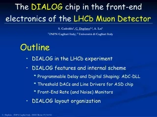
The DIALOG chip in the front-end electronics of the LHCb Muon Detector S. Cadeddu1, C. Deplano1,2, A. Lai1 1 INFN Cagliari Italy; 2 Università di Cagliari Italy Outline • DIALOG in the LHCb experiment • DIALOG features and internal scheme * Programmable Delay and Digital Shaping: ADC-DLL * Threshold DACs and Line Drivers for ASD chip * Front-End Rate (and Noise) Monitors • DIALOG layout organization C. Deplano - INFN Cagliari Italy– IEEE Rome 19/10/04
LHCb experiment Muon Detector 45 46 47 48 49 50 51 52 53 54 55 B m+m- INTERACTION BX ID DETECTION TIME DISTRIBUTION 25 ns 25 ns 25 ns 25 ns LHCb: an experiment for precise measurements of CP violation and B mesons rare decays LHC Bunch Crossing frequency ~ 40 MHz (25 ns) • Each channel of the Muon Chambers can have a different delay • Different BX • Time distribution not center inside the BX • Reasons • Particle time of flight • Different cables length • Time distribution width ~ 25 ns EFFICIENCY LOSS C. Deplano - INFN Cagliari Italy– IEEE Rome 19/10/04
LHCb experiment Muon Detector MUON CHAMBER (MWPC/GEM) F/E board F/E board ASD: CARIOCA CHIP ANALOG SHAPER DISCRIMINATOR ON DETECTOR ELECTRONICS 8 PCH 8 PCH 8 PCH 8 PCH DIALOG DIALOG CUSTOM IC DELAY AND WIDTH ADJUSTMENT LOGICAL CHANNEL GENERATION THRESHOLDS FOR ASD CHIPS 8 LCH ASD ASD SERVICE board 10m cabling (LVDS) (on crates) I2C MASTER LOW VOLTAGE CONTROLS CALIBRATION PULSES OFF DETECTOR ELECTRONICS SYNCHRONIZATION TIME (PHASE) MEASUREMENT DATA FORMATTING DATA TO MUON TRIGGER Counting Room DATA TO DAQ RECONSTRUCTION 45 46 47 48 49 50 51 52 53 54 55 B m+m- 25 ns INTERACTION BX ID DETECTION 4000 ASD 8000 DIALOG SYNC IC NSS N33-14 C. Deplano - INFN Cagliari Italy– IEEE Rome 19/10/04
DIALOG features DIALOG(Diagnostic time Adjustment and LOGics) • Programmable input signals time adjustment (31 steps of ~ 1.6 ns) • External selection or automatic calibration by DLL (settable period ~ 57 ns [17 MHz]÷ 21 ns [48 MHz]) • Programmable output signals width adjustment (8 steps of ~ 3 ns each) • Mask on every input channel • Logical Channel generation • OR2; OR4; OR8; • AND2; OR2(2AND2); OR4(4AND2) • Sixteen 24 bits rate counters • 18 different threshold signals for ASD • Internal Pattern generation • 2 ASD pulse generation signals with programmable time adjustment • I2C interface (93 registers) to configure all DIALOG tools • Triple-voted and auto-corrected register for better SEU immunity (both configuration and state machines) IBM 0.25 μm radiation tolerant technology 16 LVDS input channels 8 LVDS output channels C. Deplano - INFN Cagliari Italy– IEEE Rome 19/10/04
DIALOG Internal Scheme 16 LVDS input 8 LVDS output M A S K Prog. Delayer Prog. Dig. Shaper Logical Channel Generation MUX CAlibDLL & ADC DLL Internal pattern Calibration CLK Start/Stop 16 x 24 bits Rate counters SCL I2C Interface DIALOG Configuration registers Tst Signal SDA Address Pls0 ASD pulse generation & Delay Pulse Pls1 ASDQ Thr DAC 1 CARIOCA Threshold1 Thr DAC 1 Threshold1 … Thr DAC 2 Threshold2 Thr DAC 16 Threshold16 C. Deplano - INFN Cagliari Italy– IEEE Rome 19/10/04
Programmable Delay and Shaping PCH15 25 ns PCH9 PCH1 50 ns pulse from CARIOCA • Programmable input signals time adjustment (31 steps of ~ 1.6ns @ 40MHz) • External selection or automatic calibration by ADC-DLL • Typical max delay ~ 50 ns • Max possible delay~120 ns (@ 18 MHz) • DNL (peak to peak) < ± 0.25 LSB • Programmable output signals Digital Shaping (8 steps of ~ 3.2ns each @ 40MHz) • Typical shaping ~ 25 ns • Important to adjust the variable time width of signals (time over threshold) to the constant width of one BX cycle • DNL (peak to peak) < ± 0.2 LSB DIALOG outputs delayed by 25ns one with respect to the other • Both uses the same VCDL • External selection or automatic calibration (ADC-DLL) Time Re-aligned and shaped C. Deplano - INFN Cagliari Italy– IEEE Rome 19/10/04
DIALOG ADC-DLL 8 VCDL (matched to calibration DLL) Vctrl (after locking) ADC Ref Clock Calibration DLL VCDL 1 DAC From I2C REG VCDL 2 Code in Vout Vctrl VCDL 3 Comparator SAR and controls Code VCDL 8 Controls • Reference Clock is input only during specific calibration (initialization) runs • Locking time is < 500 ns and Conversion time is ~ 2 μs • Locking range ~ 57 ns [17 MHz]÷ 21 ns [48 MHz] • Temperature Effect: 1 ns for 20 °C (50 ps/°C)
DIALOG Thresholds Setting Tools • 2 ASD threshold setting blocks consisting of : • 8 DAC + buffer for CARIOCA • DAC: resolution 8 bit, range (625 m ÷1.2) V • Linear output driver (Rin CARIOCA ~ 24 kΩ) good linearity and uniformity for RLoad > 6.8 kΩ • DNL (peak to peak) < ± 0.5 LSB • 1 DAC + buffer for ASDQ • DAC: resolution 8 bit, range (0 ÷625 m) V • Linear output driver (Rin ASDQ ~ 1 kΩ) good linearity and uniformity for RLoad > 1 kΩ • DNL (peak to peak) < ± 0.5 LSB • 1 voltage divider + 2 buffers to give the correct voltage range to DAC • Linear output driver (Rin ~ 1 kΩ) DAC Buffer CARIOCA Buffer ASDQ C. Deplano - INFN Cagliari Italy– IEEE Rome 19/10/04
DIALOG Thresholds Setting Tools 64 threshold channels 1230 mV Max spread is 24 mV Channels profile 625 mV DNL • CARIOCA thresholds scan: 16 x 4 chip = 64 channels • Good Linearity and Uniformity • DNL profile C. Deplano - INFN Cagliari Italy– IEEE Rome 19/10/04
DIALOG front-end Rate Monitors Scaler Block for PCH EVEN PCH 0 Mux out TV out 24 bit counterTV PCH 2 out 2 PCH 2 PCH 4 24 bit counter out 4 PCH 4 PCH 6 24 bit counter Mux out 6 PCH 6 PCH 8 I2C 24 bit counter out 8 PCH 8 PCH 10 24 bit counter out 10 PCH 10 PCH 12 24 bit counter out 12 PCH 12 PCH 14 24 bit counter out 14 PCH 14 24 bit counter I2C selector • 2 Scaler blocks (one for each ASD chip) consisting of: • a 24 bits rate counter with triple-voted (TV) registers (1 channel out of 8 at a time) • seven 24 bits rate counters (one for each channel 1 ÷ 7) for test mode • Read and reset by I2C interface C. Deplano - INFN Cagliari Italy– IEEE Rome 19/10/04
DIALOG layout and pinout LVDS I2C in Reset Address LVDS I2C out 9 ASD threshold 9 ASD threshold thresholds thresholds DLL ADC core DLL ADC 8 LVDS Physical Channel 8 LVDS Physical Channel gnd gnd gnd gnd gnd gnd gnd gnd gnd gnd Scalers Pulse + Delay Lines Scalers Pulse + Delay Lines vdd vdd vdd vdd vdd vdd vdd vdd vdd vdd LVDS ASDQ pulse LVDS ASDQ pulse CARIOCA pulse 8 LVDS logical channel CARIOCA pulse • 113 pin • width 3875 mm • length 4900 mm • Power consumption ~ 50 mA at bias voltage 2.5 V • Radiation Test OK: * 250 MeV proton at PSI W/R I2C registers * Cs 137 (γ ~ 661 keV ) 1 Mrad (equivalent dose for 10 year of LHCb) C. Deplano - INFN Cagliari Italy– IEEE Rome 19/10/04
Conclusion DIALOG TB BOARD MWPC FULLY EQUIPPED CARDIAC FRONT-END BOARD • DIALOG 1.0 was completely tested under operating conditions (detector MWPC + front-end board CARDIAC) • DIALOG 1.0 is fully working and is under production at IBM C. Deplano - INFN Cagliari Italy– IEEE Rome 19/10/04