Download
1 / 19
190 likes | 397 Views
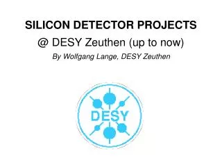
SILICON DETECTOR PROJECTS @ DESY Zeuthen (up to now) By Wolfgang Lange, DESY Zeuthen. OUTLINE. 2. Early Silicon Detectors in Zeuthen Silicon Detectors in H1 (BST, CST, FST, BST-PAD) Silicon Detectors in ZEUS (Barrel Detector) HERMES Recoil Detector Facilities and Collaborators.

E N D
SILICON DETECTOR PROJECTS @ DESY Zeuthen (up to now) By Wolfgang Lange, DESY Zeuthen
OUTLINE 2 • Early Silicon Detectors in Zeuthen • Silicon Detectors in H1 (BST, CST, FST, BST-PAD) • Silicon Detectors in ZEUS (Barrel Detector) • HERMES Recoil Detector • Facilities and Collaborators Wolfgang Lange, DESY Zeuthen: Silicon Detector Projects Kraków, 10-Oct-2003
EARLY SILICON DETECTORS 3 • Development together with Werk für Fernsehelektronik Berlin (WF) • First silicon sensors in planar technology ~ 1987 • DC coupled, 50µm pitch on 2” wafers (up to 25*25 mm2 sensors), discrete readout via fanout, electronics mounted on PCBs • Soon switched to 4” technology: 50*50mm2 sensors • DC coupled, 50µm pitch, development of the first thick film hybrid, • use of the first readout ASIC (MX-2, Stanford University) • first application: calibration of the L3-central tracking chamber @ CERN • Development together with Halbleiterwerk Frankfurt/Oder (HFO) • and Institut für Halbleiterphysik Frankfurt/Oder (IHP) • - May 1989 first own production of DELPHI type sensors (IHP FF/O) • AC coupled, 25µm pitch (one indermediate strip, polysilicon resistors), • sensors used successfully until 1993 in different experiments • 1991 we started the development of our own sensor types (strip, pad). Wolfgang Lange, DESY Zeuthen: Silicon Detector Projects Kraków, 10-Oct-2003
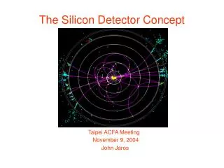
SILICON DETECTORS IN H1 - OVERVIEW 4 FST (strips) CST (strips) electron beam proton beam BST (strips, pads) proton direction = forward direction Wolfgang Lange, DESY Zeuthen: Silicon Detector Projects Kraków, 10-Oct-2003
SILICON DETECTORS IN H1 - DETAILS 5 • Three different sensor types: R-Strip, Phi-Strip, Pad • Two different readout hybrids: S-Hybrid, Pad-Hybrid VERTEX Mechanical design: Carbon fiber reinforced plastic • Modular design of all components • Design as a “plug in” device with • remotely operated contact ring • (including all media connections • for N2 and H2O) • Separate inner and outer shielding • Cable- and media connections are • pre-installed to the contact ring Wolfgang Lange, DESY Zeuthen: Silicon Detector Projects Kraków, 10-Oct-2003
S(tandard) - DETECTOR MODULE 6 • universal detector module • for front and back side • low cost design with included strip line • and heat distributing Al bottom layer • standard circuitry (using APC 128 /decoder) • optimized for low common mode and • low noise (including ground plane) • 220 modules (spares included) produced for • both FST and BST Wolfgang Lange, DESY Zeuthen: Silicon Detector Projects Kraków, 10-Oct-2003
CST BARREL (NOT ZEUTHEN [ZÜRICH] BUT H1) 7 • CST barrel consists of two layers • completely covering the vertex • (beam pipe) • Ladders consist of 6 double sided sensors • with hybrids on both sides • hybrids are equipped with radhard readout • chips APC128 (DMILL) one ladder CST hybrid Wolfgang Lange, DESY Zeuthen: Silicon Detector Projects Kraków, 10-Oct-2003
BST PAD DETECTOR 8 • For the measurement of deep inelastic scattering • one needs to trigger on such events (vertex pointing) • Background suppression for SPACAL hits • (photon background) • Four planes (disks) with pad detectors which are • read out by the trigger system of H1 (trigger level 1) • Pad detector supplies trigger patterns (“masks” or • classified tracks, L1) as well as hit patterns (level 3) • Measurement of normalized counting rates per area • allows the use as “radiation monitor” Readout chain: sensor -> detector module -> repeater (pre-processing) -> H1 readout Wolfgang Lange, DESY Zeuthen: Silicon Detector Projects Kraków, 10-Oct-2003
BST PAD DETECTOR MODULE 9 AC coupled sensors with 32 (4 * 8) pads • ASIC “PRO/A”: • 32 channels • preamp / shaper / discriminator • adjustable gain (four steps) • subtraction of neighboring • channels possible • output ‘monostable’ or • ‘time over threshold’ • input current compensation • optional • over all test feature Wolfgang Lange, DESY Zeuthen: Silicon Detector Projects Kraków, 10-Oct-2003
PERFORMANCE PAD MODULE 10 • Tuning of all modules under HERA conditions with no beam -> ‘noise counts’ • Threshold scale calibrated with MIPs in a test beam • Most critical part after design: depletion voltage of sensor • -> careful decoupling and grounding mandatory • nearly 100% trigger efficiency with tuned system • -> tracks defined already with two hits in two planes “self triggered” spectrum of MIPs (pedestal added with external trigger) Threshold scans for different depletion voltage supplies Wolfgang Lange, DESY Zeuthen: Silicon Detector Projects Kraków, 10-Oct-2003
RESULTS - strip modules 11 • Excellent performance of strip modules (S-hybrid equipped with sensors from CIS Erfurt): S/N ≥ 30 spatial resolution ≤ 12 µm Wolfgang Lange, DESY Zeuthen: Silicon Detector Projects Kraków, 10-Oct-2003
RESULTS (continued) - spatial resolution 12 • FST alignment before alignment after alignment Wolfgang Lange, DESY Zeuthen: Silicon Detector Projects Kraków, 10-Oct-2003
ACTIVITIES FOR THE ZEUS Micro Vertex Detector 13 • No development of “real silicon” but development of parts: • flex foils for the interconnection of sensors and r/o hybrids • design, production and application of special glueing • techniques for flex foils on top of silicon (tooling included) • design and production of handling tools for • double sided silicon • DC measurement of a large quantity of sensors Wolfgang Lange, DESY Zeuthen: Silicon Detector Projects Kraków, 10-Oct-2003
HERMES RECOIL DETECTOR 14 Position of Recoil Detector Recoil Detector: Detection of low momentum ‘recoil’ protons Wolfgang Lange, DESY Zeuthen: Silicon Detector Projects Kraków, 10-Oct-2003
HERMES RECOIL DETECTOR - REQUIREMENTS 15 • REQUIREMENTS ON • Silicon Sensors • Detection area about 200*100mm2 • Spatial resolution in ‘phi’ about 1mm • low quantities needed (two layers) • therefore look for sensors available • - TIGRE Sensors (MICRON Ltd. UK) • R/O ELECTRONICS (R/O Chip) • - An analog pipeline chip is needed to • accommodate the HERMES trigger. • - A dynamic range of 70 MIP ( 280 fC). • - 10 MHz readout to match the HERA • frequency. • - Prefer a chip already used in HERMES • (Lambda Wheels - HELIX 128). Wolfgang Lange, DESY Zeuthen: Silicon Detector Projects Kraków, 10-Oct-2003
HERMES RECOIL DETECTOR - R/O TECHNIQUE (1) 16 1 “MIP” = 24 000 e-/h pairs +/- “MIP” = pos/neg charge on preamp Conclusions: - Linear response over +/-10 “MIP” - Saturated at ~15 “MIP” Wolfgang Lange, DESY Zeuthen: Silicon Detector Projects Kraków, 10-Oct-2003
HERMES RECOIL DETECTOR - R/O TECHNIQUE (2) 17 Solution: charge division charge division works nicely (and can be tuned to the needs) Wolfgang Lange, DESY Zeuthen: Silicon Detector Projects Kraków, 10-Oct-2003
HERMES RECOIL DETECTOR - PROTOTYPE 18 Sensor ZEUS hybrid Wolfgang Lange, DESY Zeuthen: Silicon Detector Projects Kraków, 10-Oct-2003
FACILITIES AND COLLABORATORS 19 • At DESYZeuthen we are able to perform (class 10k clean room): • Ultrasonic wire bonding (Au, Al, down to 17.5 µm wires) • Glueing with high mechanical precision and/or special hardening procedures (silver epoxies) • Measurements of single and double sided sensors on different probe stations • long term measurements (darkness, special atmosphere: N2 or similar) • chip testing (delivered probe cards can be adapted) • additional: electronics workshop with automatic SMD placement and soldering tools • mechanical workshop with NC machining/milling • at DESY Hamburg a ‘state of the art’ programmable wire bonder • Companies / Institutions we are used to work with: • - Sensors: CiS Erfurt (D), Micron Ltd. (UK), SINTEF Oslo (N), Hamamatsu (J) • chip design: IDE AS, Oslo (N) and ASIC Laboratory of University of Heidelberg (D) • probe cards: Wentworth Deutschland GmbH, München (D) • high precision printed circuit boards: Würth GmbH, Roth am See (D), Optiprint (CH) • thick film hybrids: Elbau GmbH, Berlin (D) Wolfgang Lange, DESY Zeuthen: Silicon Detector Projects Kraków, 10-Oct-2003