Download
1 / 32
330 likes | 571 Views
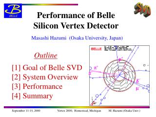
Belle SVD (Silicon Vertex Detector). Hirokazu Ishino (Tokyo Institute of Technology) for Belle SVD group Sep. 15th, 2003. Contents Introduction Performances of SVD version 1 Status and performances of upgraded SVD (SVD2) Summary. Circumference ~3km.

E N D
Belle SVD (Silicon Vertex Detector) Hirokazu Ishino (Tokyo Institute of Technology) for Belle SVD group Sep. 15th, 2003 • Contents • Introduction • Performances of SVD version 1 • Status and performances of upgraded SVD (SVD2) • Summary
Circumference ~3km The e-(8GeV) e+ (3.5GeV) beams are collided at the central position of Belle detector. beam current Lmax = 1.06 ×1034 /cm2/s ∫Ldt = 158.6/fb Introduction to Belle KEKB ring KEK, Tsukuba, Japan Belle detector the worldrecord !
The Belle Detector Aerogel Cherenkov Counter Time Of Flight Counter CsI Electromagnetic Calorimeter 3.5GeV positron beam Super Conductive Solenoid coil 8GeV electron beam KL muon detector Central Drift Chamber Silicon Vertex Detector
Physics Motivation 8GeV electron 3.5GeV positron CP eigenstate B0 or B0 (flavor tag side) U(4s) Dz ~ 200mm The CP-violation parameters can be extracted by measuring the time dependent CP-violating asymmetry. In case of It is crucial to measure the B decay vertex positions with an accuracy of several 10s micro meter. A silicon vertex detector is the most suitable.
The Belle SVD Group SVD Group Frankfurt U., U. Hawaii, Jozef Stefan Inst., Kanagawa U., KEK, Krakow INP, U. Melbourne, National Taiwan U., Niigata U., Nihon Dental U., Osaka U., Princeton U., Riken, U. Sydney, Tohoku U.,U. Tokyo, Tokyo Inst. Tech., Tokyo Metropolitan U., Toyama NCMT, U. Tsukuba, Vienna IHEP About 100 people
Ladders DSSDs Radius Length Layer per layer per ladder (mm) (mm) 1 30.0 112.5 8 2 2 45.5 10 3 168.5 3 60.5 14 4 224.5 SVD (Silicon Vertex Detector) version 1 Beam pipe radius: 20.0mm Total coverage : 23°< q < 139°in polar angle. Size of DSSD: 35.3×57.5×0.3 mm Total # of channels: 81920 VA1 chips are used for read-out Signals are digitized by FADCs equipped with DSPs DSSD (Double-sided Silicon Strip Detector)
SVD1 history • SVD1.0 • installed in winter, 1999 • VA chips with 1.2mm process (usable up to 200kRad) • read-out chips were damaged by soft X-rays • SVD1.2 • installed in fall, 1999 • a gold foil wrapped on the beam pipe to stop the X-rays • SVD1.4 • installed in summer, 2000 • VA chips with 0.8mm (function up to 1Mrad) • vacuum leak happened on the beam pipe in fall, 2002 • SVD1.6 • radiation damaged ladders were replaced • until summer in 2003
SVD1 and KEKB luminosity ~8/fb SVD1.4 ~60/fb ~90/fb SVD1.0 SVD1.2 SVD1.6
SVD1 radiation dose history The radiation dose have been measured by RadFETs. About 0.9Mrad dose have been irradiated from the installation of theSVD1.4.
SVD1 performance (Signal, Noise and S/N) elapsed days signal About 30% degradation of S/N was observed for the first layer ladders. noise S/N: 20~30 S/N bad ladders were replaced and the parameters were re-tuned VA1 parameters were re-tuned
SVD1 performance (Impact Parameter resolution) time variation of IP resolution over SVD1 operations the IP resolutions are kept throughout all periods. srf= 18.6 ⊕ 51.3/ptb sin3/2q (mm) sz= 40.8 ⊕ 43.5/ptb sin5/2q (mm) ≡ a ≡ b
Physics outcome b →ccs Acp CP = -1 sample sin2f1= 0.73±0.06 CP = +1 sample (B0gJ/y KL) sin2f1= 0.80±0.13 Dt (ps) shown at LP 2003
And... The SVD1 in the storehouse just after the un-installation. Thank you for giving us fruitful physics results!
Drawbacks of SVD1 and improvements applied to SVD2 • Radiation hardness • the 0.8mm processed VA chips can function up to 1Mrad. • utilize 0.35mm VA1TA chips: function up to 20Mrad • Improvements on vertex resolution and low Pt particle tracking. • reducethe radius of inner most layer to 20mm • increasenumber of layers to 4 • An increase in the detector acceptance • Avoidance of the break down of AC coupling • the electric short between biased and read-out strip induce large noise : 5pin holes were opened in SVD1.4 and 1.6 • utilize floating ground: isolation is made with a photo coupler • Trigger capability • New DAQ system • utilize PCs instead of VME based DSP boards in SVD1 for better performances
SVD2 components(1) support ribs bridges hybrids DSSDs Flex circuit hybrid circuit mounting 4 VA1TA chips :512 strips are readout
SVD version2 r-f view Beam pipe radius: 15.0mm Total coverage : 17°< q < 150°in polar angle: matching with CDC # of read-out channels: 110592 z VA1TA chips are used for read-out Ladders DSSDs Radius Length Layer per layer per ladder (mm) (mm) 1 20.0 156.5 6 2(1+1) 2 43.5 12 3(1+2) 236.2 3 70.0 18 5(2+3) 395.6 4 88.0 18 6(3+3) 457.8
SVD2 components(2) The flex provides the offset between the hybrids and DSSDs, reducing the radius of the inner most layer. Flex circuit hybrid side • lower capacitance than double metal • fine pitch (~50mm) with wide area (~30.3×3.3cm2) • strip yield ≳95% DSSD
SVD2 read-out (front end) L0 trigger Hold Event VA1TA: AMS 0.35mm process, radiation hardness up to 20Mrad Hold Signal • VA1 • shaping time 0.3~1.0ms • 128 channel serial read-out with 5MHz clock • TA • faster shaper (75ns or 300ns) + discriminator • 128 wired-or out put • Bias voltage and currents are generated by internal DAC (in total 680bits) Shaper 0.3~1.0ms TA shift in (L1 trigger) 5MHz serial analog out With L1 trigger, FADC start AD conversion
SVD2 read-out (back end) ladder (×54) front end back end • read-out FADC data via PCI card • sparsification • send data to the Event Builder 2m flat cable PC (×12) 30m CAT5 cable repeater system transmitting VA and TA signals 5m LVDS (×10) • Multiplex VA and TA output • Isolation of 3 levels (+40, -40, 0V) by photo couplers • control and monitor the front end. FADC (×36) • 10bit FADC, 9U VME • digitized data are stored in FIFO • find tracks base on TA hits →used for L0 and L1 trigger • provide a hit map by comparing ADC counts and thresholds on the registers for L1.5. TTM (Trigger Timing Module) (×11) • control read-out cycle of front end and FADCs • distribute triggers • monitor front end electronics • 6U VME
SVD2 read-out (back end) 10 repeaters 12 PCs 1 repeater with an internal board a PCI card a FADC board a TTM TTMs in VME
SVD2 was installed this summer after cabling SVD2 is carried near Belle cable covers SVD2 is going in Belle beam pipe
SVD2 performances (VA gain and detector noise) noise measurements VA1 gain measurements p side 2 DSSDs 1 DSSD slope -8fC +12fC 3 DSSDs 3 DSSDs (layer 4) ~80mV/fC 6% (5% no calib. input, 1% dead)
SVD2 performances (a cosmic ray muon track) r-f view z-y view green marks: strip hits boxes : TA hits
SVD2 performances (S/N) cluster energy: ~18000 electrons at the Landau peak for all ladder types p -side 8000 50000 n -side Although the detector size of SVD2 is larger than that of SVD1, S/N of SVD2 is comparablewith that of SVD1. -50000 -8000 cluster energy (electrons)
SVD2 performances (alignment and intrinsic resolution) residual distributions before alignment after alignment x (rf) intrinsic resolutions sx: 12.0±0.4mm Pitch size : 50mm +300mm -300mm +300mm -300mm z sz: 22.3±0.8mm Pitch size : 75mm -300mm +300mm +300mm -300mm
SVD2 performances (hit efficiency) a muon track hit or not? DSSDs expected hit efficiencies are obtained the inefficiencies are due to flex deficit, miss-wire bonding and mulfunction of read-out chips
7% strips: 5%:no calib. input 2%: TA dead SVD2 performances (TA performances) TA thresholds of 55296 strips (only p-side) were tuned using VA calibration input pulses. threshold distribution threshold curves of 8strips Number of TA hits threshold (electrons) input pulse height ~12000 electrons on average
SVD2 TA hit efficiency Strip hits associated with muon tracks are used. strip charge (electrons) overall TA hit efficiency: 69.3% We should make further efforts to lower the threshold. strip charge (electrons)
processing speed (Hz) SVD2 DAQ performance • In SVD2, a PC based DAQ system was developed: • for managing 3 times data flow compared with SVD1 • the required processing speed should be greater than 1kHz • We measured the speed by changing sparsification thresholds to vary the occupancy, • the speed : ~1.3kHz @ 5% occu. • data size: 10kB/event @5% occu. occupancy data processing speed of the DAQ system including not only read-out PCs but also the Belle event builder
Summary • SVD1 had worked excellently. • About 1Mard dose had been irradiated. • Although S/N had degraded by about 30%, IP resolutions are stable throughout 3 year operation. • SVD2 was installed this summer. • Basic functions of VA1TA chips are working very well. • Basic performances were checked using cosmic ray muon events: • S/N was obtained to be 20 to 40. • Hit efficiencies were measured to be 95~98%. • With the alignment of the SVD2, intrinsic resolutions were estimated to be 12mm for r-f and 22mm for z side. • SVD2 DAQ system is able to process the data at a 1.3kHz trigger rate. • Schedule • integration of L0, L1 and L1.5 trigger by the middle of Oct. • Beam injection will start mid. of Oct, hope the first collision data.