Download
1 / 29
290 likes | 504 Views
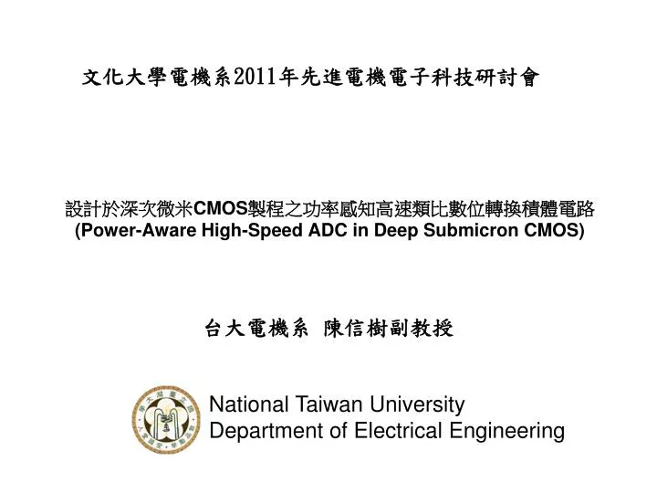
文化大學電機系 2011 年先進電機電子科技研討會. 設計於深次微米 CMOS 製程之功率感知高速類比數位轉換積體電路 (Power-Aware High-Speed ADC in Deep Submicron CMOS). Outline. Motivation H igh-speed ADC IC design example Digitally-assisted algorithm and architecture Circuit implementation Experimental results Summary.

E N D
文化大學電機系2011年先進電機電子科技研討會文化大學電機系2011年先進電機電子科技研討會 設計於深次微米CMOS製程之功率感知高速類比數位轉換積體電路(Power-Aware High-Speed ADC in Deep Submicron CMOS)
Outline • Motivation • High-speed ADC IC design example • Digitally-assisted algorithm and architecture • Circuit implementation • Experimental results • Summary
High-Speed ADC Applications • Ref [1]
Power-Aware High-Speed ADC Trends • Power / Energy • Higher resolution requires more energy to achieve. • Speed / Bandwidth • Resolution and speed are trade-offs. • Bottleneck • SAR architecture saves power and chip area, but speed is limited by its conversion algorithm. • Pipelined architecture achieves high speed by concurrent operations, but OPAs consume considerable power. • Digitally assisted ADCs • Digitally assisted algorithm alleviates analog circuit requirement; therefore, it takes advantages of advanced processes to trade little digital power to gain the benefits from analog part.
High-Speed ADC Energy vs. SNDR • Energy is proportional to resolution (SNDR). • FOM (Power / (Sample rate * 2ENOB)) is an indicator to compare different ADC designs. • State-of-the-art ADC designs approach 10fJ/c.s. Current world record is 4fJ/c.s. • Ref [2]
High-Speed ADC Bandwidth vs. SNDR • Bandwidth is inverse proportional to resolution (SNDR). • State-of-the-art high-speed high-resolution ADCs are limited by clock jitter around 0.1psrms. • Ref [2]
Experiment 1 - Low-Power High-Speed Two-Step ADC • Rearrange the timing of two-channel MDACs and apply a self-timing technique to alleviate comparator comparison time and charge injection disturbance • Slightly increases CADC accuracy to ease OPA signal swing design • Ref [3]
Experiment 2 - Low-Power High-Speed Sub-range SAR ADC • Relieve MSB accuracy requirement by the sub-range concept with overlapping • Reduce total input capacitance by using the double-unit-sized coupling-capacitor • Ref [4]
Experiment 3 - Low-Power High-Speed SAR ADC • Attain high conversion speed by adopting non-constant-radix switching method • Compared to conventional non-binary designs, its DAC implementation is simpler.
Experiment 4 - Low-Power High-Speed Pipelined ADC • Achieve high speed with a low-gain OPA by using digitally-assisted architecture, thus the OPAs have excellent power efficiency • A simple gain-error self calibration method without external precise references requires only 168 calibration clock cycles. • Ref [5]
Digitally-Assisted High-Speed ADC Example (Experiment 4) • Digitally assisted architecture is future trend to achieve excellent power efficiency. • 10b, several hundreds MS/s Pipeline ADCs are widely used in wireless and cloud computing systems but suffer from OPA design in deep submicron CMOS processes. • Decreased OPA DC gain • Smaller signal swing
Pipeline ADC Accuracy • OPA gain • Less Ro of MOSFET in advanced technologies • Reduced gain from each stage of OPA • More gain stages introduce poles and decrease bandwidth. • For 10b accuracy, the 1st stage MDAC requires 66dB OPA DC gain. • Capacitor mismatch • Raw matching can attain 10b accuracy, not an issue!
Closed-Loop Gain Error • For finite A, closed-loop gain ACL is smaller than ideal gain, 1/b. • Gain error can be compensated by adjustingb.
MDAC Gain Error • Due to finite A, closed-loop gain is less than ideal value of 4. • b adjustment is proposed to correct MDAC gain error.
Proposed MDAC with a Calibration Capacitor • A calibration capacitor, Ccal, is added as a positive feedback to adjust b. • Closed-loop gain can achieve 10b accuracy with low DC gain A of 30dB.
Self-Calibrated Algorithm (1) • Self-calibrated procedure starts with the last stage MDAC. • After MDAC is calibrated, it is treated as “ideal” MDAC. • Ideal MDACs subtract 3Vref/8 and then multiply 4. • Under-Calibration MDAC samples Vref/8 and then multiplies 4.
Self-Calibrated Algorithm (2) – Gain Error • Output is Vref/2 when no gain error • Using successive approximation method with iterations, the closed-loop gain reaches 4 with 10b accuracy.
Proposed ADC Architecture • On-chip foreground analog self-calibrated technique • Gain errors of first three stages are calibrated
Calibration Step • 128 calibration steps • Each step affects 0.14 % of MDAC gain (~4) with OPA gain of 40dB
Calibration Range • Ccal in this work can calibrate OPA with a minimum DC gain of 30dB
OPA • Use small L to increase bandwidth without considering gain • Calibration mode has more compensation capacitance • Simulation results: DC gain 40dB, closed-loop BW 1.36GHz
Chip Micrograph • 0.21mm2 active area in 90 nm low-power CMOS
Measured DNL Before calibration After calibration • Before calibration: +1.7 / -1.0 LSB • After calibration: +0.7/-0.6 LSB
Measured INL Before calibration After calibration • Before calibration: +15.6/-15.2 LSB • After calibration: +0.8/-0.9 LSB
Measured Dynamic Performance • At low Fin, SNDR ≈ 54.2dB, ENOB ≈ 8.7bit • At Nyquist Fin, SNDR ≈ 51.2dB, ENOB ≈ 8.2bit • ERBW ≈ 160MHz
Measured FFT • SNDR ≈ 52.8dB and SFDR ≈ 57.8dB when Fs = 320MHz and Fin = 128MHz
Summary • A simple self-calibrated algorithm is proposed to correct gain error resulting from low gain OPA in deep submicron CMOS. • The self-calibrated process does not require a precise external reference and can be done within only 168 clock cycles. • Smallest active area of 0.21mm2 in 90nm CMOS including calibration circuit • The prototype ADC achieves 320MS/s conversion rate, 8.7 ENOB and only consumes 42mW. Nice power efficiency is obtained. • Power efficiency is the key to high-speed ADC IC designs.
Reference [1] http://www.analog.com/library/analogdialogue/archives/39-06/architecture.html [2] B. Murmann, "ADC Performance Survey 1997-2010," [Online]. Available: http://www.stanford.edu/~murmann/adcsurvey.html [3] H. Chen et al., “A 1-GS/s 6-Bit Two-Channel Two-Step ADC in 0.13-mm CMOS,” IEEE J. Solid-State Circuits, vol. 44, no. 11, pp. 3051-3059, Nov. 2009. [4] H. Chen et al., “A 3mW 12b 10MS/s Sub-Range SAR ADC” in IEEE Asian Solid-State Circuits Conf. Dig. Tech. Papers, Taipei, Taiwan, pp. 153-156, Nov. 2009. [5] H. Chen et al., “A 10b 320MS/s Self-Calibrated Pipeline ADC” in IEEE Asian Solid-State Circuits Conf. Dig. Tech. Papers, Peking, China, pp. 173-176, Nov. 2010. [6] B. Razavi and B. A. Wooley, “Design Techniques for High-Speed, High-Resolution Comparators,” IEEE J. Solid-State Circuits, vol. 27, no. 12, pp. 1916-1926, Dec. 1992. [7] A. Verma and B. Razavi, ”A 10b 500MHz 55mW CMOS ADC,” IEEE J. Solid-State Circuits, vol. 44, no. 11, pp. 3039-3050, Nov. 2009. [8] B. Hernes et al.,”A 92.5mW 205MS/s 10b Pipeline IF ADC Implemented in 1.2V/3.3V 0.13mm CMOS,” ISSCC Dig. Tech. Papers, pp. 462-463, Feb. 2007.