Static CMOS Logic
Static CMOS Logic. ECE442: Digital Electronics. CMOS Circuit Styles. Static complementary CMOS - except during switching, output connected to either V DD or GND via a low-resistance path high noise margins full rail to rail swing V OH and V OL are at V DD and GND, respectively

Static CMOS Logic
E N D
Presentation Transcript
Static CMOS Logic ECE442: Digital Electronics
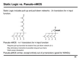
CMOS Circuit Styles • Static complementary CMOS - except during switching, output connected to either VDD or GND via a low-resistance path • high noise margins • full rail to rail swing • VOH and VOL are at VDD and GND, respectively • low output impedance, high input impedance • no steady state path between VDD and GND (no static power consumption) • delay a function of load capacitance and transistor resistance • comparable rise and fall times (under the appropriate transistor sizing conditions) • Dynamic CMOS - relies on temporary storage of signal values on the capacitance of high-impedance circuit nodes • simpler, faster gates • increased sensitivity to noise
PMOS transistors only pull-up: make a connection from VDD to F when F(In1,In2,…InN) = 1 pull-down: make a connection from F to GND when F(In1,In2,…InN) = 0 NMOS transistors only Static Complementary CMOS • Pull-up network (PUN) and pull-down network (PDN) VDD In1 In2 PUN … InN F(In1,In2,…InN) In1 In2 PDN … InN PUN and PDN are dual logic networks
CL CL CL CL Threshold Drops VDD VDD PUN S D VDD D S 0 VDD 0 VDD - VTn VGS VDD 0 VDD |VTp| PDN VGS D S VDD S D
Construction of PDN • NMOS devices in series implement a NAND function • NMOS devices in parallel implement a NOR function A • B A B A + B A B
Dual PUN and PDN • PUN and PDN are dual networks • DeMorgan’s theorems A + B = A • B [!(A + B) = !A • !B or !(A | B) = !A & !B] A • B = A + B [!(A • B) = !A + !B or !(A & B) = !A | !B] • a parallel connection of transistors in the PUN corresponds to a series connection of the PDN • Complementary gate is naturally inverting (NAND, NOR, AOI, OAI) • Number of transistors for an N-input logic gate is 2N
CMOS NAND A B A • B A B A B
CMOS NOR B A A + B A B A B
B A C D Complex CMOS Gate OUT = (D + A • (B + C))* A D B C
A B C Example: OAI Logic A C B X = (C • (A + B))* C A B
A B C D Example: OAI Logic A C B D X = ((A+B)•(C+D))* C D A B
XNOR/XOR Implementation XNOR XOR A A A B A B B B A A B B A B A B • How many transistors in each?
C*out = C*in & (A* | B*) | (!A & !B) !Sum= Cout & (!A | !B | !Cin) | (!A & !B & !Cin) B A B B A B Cin A A Cin !Cout !Sum Cin A Cin A B B A B Cin A B Sum= !Cout & (A | B | Cin) | (A & B & Cin) Cout = Cin & (A | B) | (A & B) Static CMOS Full Adder Circuit