Error Analysis and Management for MLC NAND Flash Memory
870 likes | 918 Views
Learn about experimental characterization, error models, and techniques for improving reliability & endurance in NAND flash memory. Discover recent results and industry challenges.

Error Analysis and Management for MLC NAND Flash Memory
E N D
Presentation Transcript
Error Analysis and Management for MLC NAND Flash Memory Onur Mutlu onur@cmu.edu (joint work with Yu Cai, Gulay Yalcin, Erich Haratsch, Ken Mai, Adrian Cristal, Osman Unsal) August 7, 2014 Flash Memory Summit 2014, Santa Clara, CA
Executive Summary • Problem: MLC NAND flash memory reliability/endurance is a key challenge for satisfying future storage systems’ requirements • Our Goals: (1) Build reliable error models for NAND flash memory via experimental characterization, (2) Develop efficient techniques to improve reliability and endurance • This talk provides a “flash” summary of our recent results published in the past 3 years: • Experimental error and threshold voltage characterization [DATE’12&13] • Retention-aware error management [ICCD’12] • Program interference analysis and read reference V prediction [ICCD’13] • Neighbor-assisted error correction [SIGMETRICS’14]
Agenda • Background, Motivation and Approach • Experimental Characterization Methodology • Error Analysis and Management • Characterization Results • Retention-Aware Error Management • Threshold Voltage and Program Interference Analysis • Read Reference Voltage Prediction • Neighbor-Assisted Error Correction • Summary
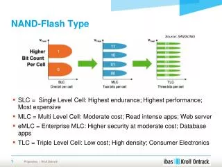
Evolution of NAND Flash Memory • Flash memory is widening its range of applications • Portable consumer devices, laptop PCs and enterprise servers CMOS scaling More bits per Cell Seaung Suk Lee, “Emerging Challenges in NAND Flash Technology”, Flash Summit 2011 (Hynix)
Flash Challenges: Reliability and Endurance • P/E cycles (provided) A few thousand • P/E cycles (required) Writing the full capacity of the drive 10 times per day for 5 years (STEC) > 50k P/E cycles E. Grochowski et al., “Future technology challenges for NAND flash and HDD products”, Flash Memory Summit 2012
NAND Flash Memory is Increasingly Noisy Read Write Noisy NAND
Future NAND Flash-based Storage Architecture Raw Bit Error Rate Uncorrectable BER < 10-15 Memory Signal Processing Noisy Error Correction Lower High Better Our Goals: Build reliable error models for NAND flash memory Design efficient reliability mechanisms based on the model
NAND Flash Error Model Write Read Noisy NAND Experimentally characterize and model dominant errors Cai et al., “Error Patterns in MLC NAND Flash Memory: Measurement, Characterization, and Analysis””, DATE 2012 • Neighbor page program (c-to-c interference) Read Write • Erase block • Program page • Retention Cai et al., “Threshold voltage distribution in MLC NAND Flash Memory: Characterization, Analysis, and Modeling”, DATE 2013 Cai et al., “Program Interference in MLC NAND Flash Memory: Characterization, Modeling, and Mitigation”, ICCD 2013 Cai et al., “Neighbor-Cell Assisted Error Correction in MLC NAND Flash Memories”, SIGMETRICS 2014 Cai et al., “Flash Correct-and-Refresh: Retention-aware error management for increased flash memory lifetime”, ICCD 2012 Cai et al., “Error Analysis and Retention-Aware Error Management for NAND Flash Memory, ITJ 2013
Our Goals and Approach • Goals: • Understand error mechanisms and develop reliable predictive models for MLC NAND flash memory errors • Develop efficient error management techniques to mitigate errors and improve flash reliability and endurance • Approach: • Solid experimental analyses of errors in real MLC NAND flash memory drive the understanding and models • Understanding, models and creativity drive the new techniques
Agenda • Background, Motivation and Approach • Experimental Characterization Methodology • Error Analysis and Management • Main Characterization Results • Retention-Aware Error Management • Threshold Voltage and Program Interference Analysis • Read Reference Voltage Prediction • Neighbor-Assisted Error Correction • Summary
USB Daughter Board USB Jack HAPS-52 Mother Board Virtex-II Pro (USB controller) NAND Daughter Board Experimental Testing Platform 3x-nm NAND Flash Virtex-V FPGA (NAND Controller) [Cai+, FCCM 2011, DATE 2012, ICCD 2012, DATE 2013, ITJ 2013, ICCD 2013, SIGMETRICS 2014] Cai et al., FPGA-based Solid-State Drive prototyping platform, FCCM 2011.
NAND Flash Usage and Error Model Read Errors Retention Errors Program Errors Erase Errors Read Errors Retention Errors Start P/E cycle n P/E cycle i P/E cycle 0 Erase Block Program Page (Page0 - Page128) … Retention1 (t1 days) Retention j (tj days) Read Page Read Page … … End of life
Methodology: Error and ECC Analysis • Characterized errors and error rates of 3x and 2y-nm MLC NAND flash using an experimental FPGA-based platform • [Cai+, DATE’12, ICCD’12, DATE’13, ITJ’13, ICCD’13, SIGMETRICS’14] • Quantified Raw Bit Error Rate (RBER) at a given P/E cycle • Raw Bit Error Rate: Fraction of erroneous bits without any correction • Quantified error correction capability (and area and power consumption) of various BCH-code implementations • Identified how much RBER each code can tolerate how many P/E cycles (flash lifetime) each code can sustain
NAND Flash Error Types • Four types of errors [Cai+, DATE 2012] • Caused by common flash operations • Read errors • Erase errors • Program (interference) errors • Caused by flash cell losing charge over time • Retention errors • Whether an error happens depends on required retention time • Especially problematic in MLC flash because threshold voltage window to determine stored value is smaller
Agenda • Background, Motivation and Approach • Experimental Characterization Methodology • Error Analysis and Management • Main Characterization Results • Retention-Aware Error Management • Threshold Voltage and Program Interference Analysis • Read Reference Voltage Prediction • Neighbor-Assisted Error Correction • Summary
Observations: Flash Error Analysis retention errors • Raw bit error rate increases exponentially with P/E cycles • Retention errors are dominant (>99% for 1-year ret. time) • Retention errors increase with retention time requirement Raw Bit Error Rate P/E Cycles Cai et al., Error Patterns in MLC NAND Flash Memory, DATE 2012.
Retention Error Mechanism LSB/MSB Stress Induced Leakage Current (SILC) • Electron loss from the floating gate causes retention errors • Cells with more programmed electrons suffer more from retention errors • Threshold voltage is more likely to shift by one window than by multiple Floating Gate REF2 REF1 REF3 10 00 11 01 Vth Fully programmed Erased
Retention Error Value Dependency • Cells with more programmed electrons tend to suffer more from retention noise (i.e. 00 and 01) 01 10 00 01
More on Flash Error Analysis • Yu Cai, Erich F. Haratsch, Onur Mutlu, and Ken Mai,"Error Patterns in MLC NAND Flash Memory: Measurement, Characterization, and Analysis"Proceedings of the Design, Automation, and Test in Europe Conference (DATE), Dresden, Germany, March 2012. Slides (ppt)
Agenda • Background, Motivation and Approach • Experimental Characterization Methodology • Error Analysis and Management • Main Characterization Results • Retention-Aware Error Management • Threshold Voltage and Program Interference Analysis • Read Reference Voltage Prediction • Neighbor-Assisted Error Correction • Summary
Flash Correct-and-Refresh (FCR) • Key Observations: • Retention errors are the dominant source of errors in flash memory [Cai+ DATE 2012][Tanakamaru+ ISSCC 2011] limit flash lifetime as they increase over time • Retention errors can be corrected by “refreshing” each flash page periodically • Key Idea: • Periodically read each flash page, • Correct its errors using “weak” ECC, and • Either remap it to a new physical page or reprogram it in-place, • Before the page accumulates more errors than ECC-correctable • Optimization: Adapt refresh rate to endured P/E cycles Cai et al., Flash Correct and Refresh, ICCD 2012.
FCR: Two Key Questions • How to refresh? • Remap a page to another one • Reprogram a page (in-place) • Hybrid of remap and reprogram • When to refresh? • Fixed period • Adapt the period to retention error severity
In-Place Reprogramming of Flash Cells Floating Gate Floating Gate Voltage Distribution for each Stored Value • Pro: No remapping needed no additional erase operations • Con: Increases the occurrence of program errors Retention errors are caused by cell voltage shifting to the left ISPP moves cell voltage to the right; fixes retention errors
Normalized Flash Memory Lifetime 46x 4x Lifetime of FCR much higher than lifetime of stronger ECC Adaptive-rate FCR provides the highest lifetime
Energy Overhead • Adaptive-rate refresh: <1.8% energy increase until daily refresh is triggered 7.8% 5.5% 2.6% 1.8% 0.4% 0.3% Refresh Interval
More Detail and Analysis on FCR • Yu Cai, Gulay Yalcin, Onur Mutlu, Erich F. Haratsch, Adrian Cristal, Osman Unsal, and Ken Mai,"Flash Correct-and-Refresh: Retention-Aware Error Management for Increased Flash Memory Lifetime"Proceedings of the 30th IEEE International Conference on Computer Design (ICCD), Montreal, Quebec, Canada, September 2012. Slides (ppt)(pdf)
Agenda • Background, Motivation and Approach • Experimental Characterization Methodology • Error Analysis and Management • Main Characterization Results • Retention-Aware Error Management • Threshold Voltage and Program Interference Analysis • Read Reference Voltage Prediction • Neighbor-Assisted Error Correction • Summary
Key Questions • How does threshold voltage (Vth) distribution of different programmed states change over flash lifetime? • Can we model it accurately and predict the Vth changes? • Can we build mechanisms that can correct for Vth changes? (thereby reducing read error rates)
Threshold Voltage Distribution Model Characterized on 2Y-nm chips using the read-retry feature Gaussian distribution with additive white noise As P/E cycles increase ... • Distribution shifts to the right • Distribution becomes wider Cai et al., Threshold Voltage Distribution in MLC NAND Flash Memory, DATE 2013.
Threshold Voltage Distribution Model • Vth distribution can be modeled with ~95% accuracy as a Gaussian distribution with additive white noise • Distortion in Vth over P/E cycles can be modeled and predicted as an exponential function of P/E cycles • With more than 95% accuracy
More Detail on Threshold Voltage Model • Yu Cai, Erich F. Haratsch, Onur Mutlu, and Ken Mai,"Threshold Voltage Distribution in MLC NAND Flash Memory: Characterization, Analysis and Modeling"Proceedings of the Design, Automation, and Test in Europe Conference (DATE), Grenoble, France, March 2013. Slides (ppt)
Program Interference Errors • When a cell is being programmed, voltage level of a neighboring cell changes (unintentionally) due to parasitic capacitance coupling can change the data value stored • Also called program interference error • Causes neighboring cell voltage to increase (shift right) • Once retention errors are minimized, these errors can become dominant
How Current Flash Cells are Programmed • Programming 2-bit MLC NAND flash memory in two steps Vth 1 0 LSB Program Temp (0x) ER (11) ER (11) P2 (00) ER (11) P3 (01) P1 (10) Vth 1 0 0 1 MSB Program Vth
Basics of Program Interference (n+1,j) (n+1,j+1) (n+1,j-1) MSB:6 WL<2> ∆Vxy ∆Vxy ∆Vxy ∆Vxy ∆Vy ∆Vy LSB:3 MSB:4 WL<1> LSB:1 Victim Cell ∆Vx ∆Vx (n,j) MSB:2 WL<0> LSB:0 (n-1,j-1) (n-1,j) (n-1,j+1)
Traditional Model for Vth Change (n+1,j) (n+1,j+1) (n+1,j-1) • Traditional model for victim cell threshold voltage change MSB:6 WL<2> ∆Vxy ∆Vxy ∆Vy LSB:3 MSB:4 WL<1> LSB:1 Victim Cell ∆Vx ∆Vx (n,j) MSB:2 WL<0> LSB:0 (n-1,j-1) (n-1,j) (n-1,j+1) Not accurate and requires knowledge of coupling caps!
Our Goal and Idea • Develop a new, more accurate and easier to implement model for program interference • Idea: • Empirically characterize and model the effect of neighbor cell Vth changes on the Vth of the victim cell • Fit neighbor Vth change to a linear regression model and find the coefficients of the model via empirical measurement Can be measured
Developing a New Model via Empirical Measurement • Feature extraction for Vth changes based on characterization • Threshold voltage changes on aggressor cell • Original state of victim cell • Enhanced linear regression model • Maximum likelihood estimation of the model coefficients (vector expression)
Effect of Neighbor Voltages on the Victim • Immediately-above cell interference is dominant • Immediately-diagonal neighbor is the second dominant • Far neighbor cell interference exists • Victim cell’s Vth has negative effect on interference Cai et al., Program Interference in MLC NAND Flash Memory, ICCD 2013
New Model for Program Interference (n+1,j) (n+1,j+1) (n+1,j-1) ∆Vxy ∆Vxy ∆Vxy ∆Vxy ∆Vy ∆Vy MSB:6 WL<2> LSB:3 MSB:4 WL<1> Victim Cell ∆Vx ∆Vx LSB:1 (n,j) MSB:2 WL<0> LSB:0 (n-1,j-1) (n-1,j) (n-1,j+1) Cai et al., Program Interference in MLC NAND Flash Memory, ICCD 2013
Model Accuracy Characterized on 2Y-nm chips using the read-retry feature (x,y)=(measured before interference, measured after interference) Ideal if no interference Interference causes systematic Vth shift (x,y)=(measured before interference, predicted with model) Ideal if prediction is 100% accurate Model corrects for the Vth shift: 96.8% acc.
Many Other Results in the Paper • Yu Cai, Onur Mutlu, Erich F. Haratsch, and Ken Mai,"Program Interference in MLC NAND Flash Memory: Characterization, Modeling, and Mitigation"Proceedings of the 31st IEEE International Conference on Computer Design (ICCD), Asheville, NC, October 2013. Slides (pptx)(pdf)Lightning Session Slides (pdf)
Agenda • Background, Motivation and Approach • Experimental Characterization Methodology • Error Analysis and Management • Main Characterization Results • Retention-Aware Error Management • Threshold Voltage and Program Interference Analysis • Read Reference Voltage Prediction • Neighbor-Assisted Error Correction • Summary
Mitigation: Applying the Model • So, what can we do with the model? • Goal: Mitigate the effects of program interference caused voltage shifts
Optimum Read Reference for Flash Memory • Read reference voltage affects the raw bit error rate • There exists an optimal read reference voltage • Predictable if the statistics (i.e. mean, variance) of threshold voltage distributions are characterized and modeled f(x) g(x) f(x) g(x) State-A State-B State-A State-B Vth Vth v0 v1 vref v’ref v0 v1
Optimum Read Reference Voltage Prediction • Vth shift learning (done every ~1k P/E cycles) • Program sample cells with known data pattern and test Vth • Program aggressor neighbor cells and test victim Vth after interference • Characterize the mean shift in Vth (i.e., program interference noise) • Optimum read reference voltage prediction • Default read reference voltage + Predicted mean Vth shift by model Vth shift After program interference
Effect of Read Reference Voltage Prediction • Read reference voltage prediction reduces raw BER (by 64%) and increases the P/E cycle lifetime (by 30%) 30% lifetime improvement Raw bit error rate 32k-bit BCH Code (acceptable BER = 2x10⁻³) No read reference voltage prediction With read reference voltage prediction
More on Read Reference Voltage Prediction • Yu Cai, Onur Mutlu, Erich F. Haratsch, and Ken Mai,"Program Interference in MLC NAND Flash Memory: Characterization, Modeling, and Mitigation"Proceedings of the 31st IEEE International Conference on Computer Design (ICCD), Asheville, NC, October 2013. Slides (pptx)(pdf)Lightning Session Slides (pdf)
Agenda • Background, Motivation and Approach • Experimental Characterization Methodology • Error Analysis and Management • Main Characterization Results • Retention-Aware Error Management • Threshold Voltage and Program Interference Analysis • Read Reference Voltage Prediction • Neighbor-Assisted Error Correction • Summary
Goal • Develop a better error correction mechanism for cases where ECC fails to correct a page
Observations So Far • Immediate neighbor cell has the most effect on the victim cell when programmed • A single set of read reference voltages is used to determine the value of the (victim) cell • The set of read reference voltages is determined based on the overall threshold voltage distribution of all cells in flash memory