Download
1 / 32
350 likes | 749 Views
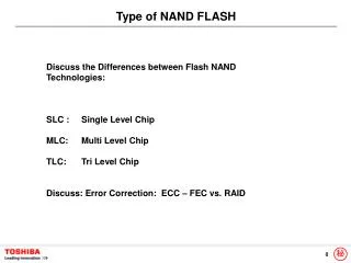
Type of NAND FLASH. Discuss the Differences between Flash NAND Technologies: SLC : Single Level Chip MLC: Multi Level Chip TLC: Tri Level Chip Discuss: Error Correction: ECC – FEC vs. RAID. Type of NAND FLASH.

E N D
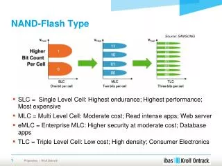
Type of NAND FLASH Discuss the Differences between Flash NAND Technologies: SLC : Single Level Chip MLC: Multi Level Chip TLC: Tri Level Chip Discuss: Error Correction: ECC – FEC vs. RAID
Type of NAND FLASH Flash memory (both NOR and NAND types)was invented by TOSHIBA /Dr. Fujio Masuoka circa 1980.
Type of NAND FLASH http://www.slideshare.net/Flashdomain/toshiba-america-electronic-components-inc-flash-memory FLASH NAND: NOW CELEBRATING 25 YEARS. NAND was invented to replace HDD “Technology” by having a device that can continue to operate even in failure mode FLASH needs its own Dedicated system Flash Controller. A Data controller to emulate the HDD Sector//Header Controller is the Host interface creating HDD commands into Flash memory Also to include error detect/defect/replacing sector blocks without shutting down or rebuilding. Made to prevent hitting same physical cells. ( Called Wear leveling)
Type of NAND FLASH Difference Between Single Level Cell and Multi Level Cell Flash Memory
Type of NAND FLASH SSD is usually MLC Based Single DIE: 64 Gb 8 Die in a Package 8x 64Gb= 512 Gbits. Offer better Density Improvements and Life cycle Retention R/W Endurance Algorithm management is needed for MLC. As MLC Noise Interference is greater when writing more information to a cell ( Not the case for SLC). To manage Noise interference between adjacent Cells Step Voltages is applied to minimize noise interference.
Type of NAND FLASH IOPS: HDD = 15 k RPM 10 K HDD =150 IOPS vs 4000 IOPS Calculations on MLC HDD Random Reads Vs. FLASH Sequential Reads HDD: Writes over Vs FLASH: Erase before Write (NAND Can Always Read instantly Anywhere from Chip)
Type of NAND FLASH The image above is a NAND array with ~16 billion transistors (one transistor is required per cell), i.e. 16 gigabits (Gb). This array can be turned into either SLC, MLC, or TLC. Current Production” Single Die” is now a 128Gb Chips @ 19 Nm For SLC, MCL or TLC.
Type of NAND FLASH Density Improvements : Current 19Nm down to 10Nm in 7 years? Future 3D NAND Flash by 2015 by Layer stack of 15
Type of NAND FLASH For Video Server: Toshiba Creates a High Level “RAID” Data recovery with Redundancy ECC and FEC. Error Correction Coding Forward Error Correction Allowing continued playout during Chip errors By pre calculating the Parity Bits to the RAW Data
DATA compensation technique 1. Toshiba unique FLASH Memory Controller Toshibahas own unique FLASH memory controller which handles Wear-leveling and RAID. The FLASH memory controller manages device wear-leveling so that the writing time into each cell across all chip devices is completely equalized. The alarm threshold for too much writing onto a certain device is controlled. The Memory controller also Manages “BAD BLOCK” to avoid to use, yet will still continue to operate. The number of memory boards under one memory controller is 4 cards in normal configuration, 5 in RAID configuration.
DATA compensation technique • 2. Error correction method • OAM FLASH has a Two layer error correction method. Lower layer is done by • Reed-Solomon (32,30) in each memory board and • High layer FEC Reed-Solomon (240,224) in memory controller. • Low layer error correction, Reed-Solomon (32,30) • The unit of data writing into FLASH memory is 32 bytes, 1 byte is written into • 1device, 32 FLASH memory devices are written in parallel. 32 bytes data • include 2 bytes Reed-Solomon code. Using this RS code, 1 byte error correction, • that is 1 device failure, is detected and corrected in each memory board. Memory • board reports to memory controller that “low layer error “ was made corrected • Therefore memory controller knows 1 device failure in memory board but does • nothing because read data has been already corrected. Up to 8 device failures • can be corrected by low layer error correction because of depth expansion. The • number of correctable device failures depends on the location of device failures.
DATA compensation technique Memory board
DATA compensation technique (2) High layer error correction, Reed-Solomon (240,224) Memory controller also adds 16 bytes Reed-Solomon code into every 224 bytes data. 30bytes data comes from each memory board at 1 cycle. To get 240 bytes it takes 2 cycles. 30bytes x 2cycles x 4 boards = 240bytes
DATA compensation technique 240 bytes data that includes 224 bytes original data and 16 bytes RS code is separated and written in/read from 4 memory board for 2 access cycles. 120 bytes to/from 4 memory boards in 1 access cycle, 30 bytes to/from 1 memory board in 1 access cycle.
DATA compensation technique Reed-Solomon (240,224) can correct 8 bytes error in 240 bytes. There should be 2 bytes error data in 240 bytes in the case that 1 device failure occurs because two sets of 1 byte error appear according to two read cycles in 240 bytes read operation. So memory controller can correct 4 device failures by Reed-Solomon (224,240). Up to 32, 4 x 8, device failures can be corrected.
DATA compensation technique 3. RAID The number of memory boards under one memory controller is 4 in normal configuration, 5 in RAID configuration. Parity data will be written in one additional memory board in RAID configuration.
DATA compensation technique Under RAID configuration, the memory controller recognizes new memory board when inserted into failed memory slot, the content data which was in that location is re-created from the 4 boards using parity. Data is now rapidly recovered onto the new memory board.