Download
1 / 30
300 likes | 338 Views
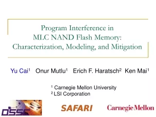
Program Interference in MLC NAND Flash Memory: Characterization, Modeling, and Mitigation. Yu Cai 1 Onur Mutlu 1 Erich F. Haratsch 2 Ken Mai 1. 1 Carnegie Mellon University 2 LSI Corporation. Flash Challenges: Reliability and Endurance. P/E cycles (provided). A few thousand.

E N D
Program Interference in MLC NAND Flash Memory: Characterization, Modeling, and Mitigation Yu Cai1Onur Mutlu1Erich F. Haratsch2 Ken Mai1 1 Carnegie Mellon University 2 LSI Corporation
Flash Challenges: Reliability and Endurance • P/E cycles (provided) A few thousand • P/E cycles (required) Writing the full capacity of the drive 10 times per day for 5 years (STEC) > 50k P/E cycles E. Grochowski et al., “Future technology challenges for NAND flash and HDD products”, Flash Memory Summit 2012
NAND Flash Memory is Increasingly Noisy Read Write Noisy NAND
Future NAND Flash-based Storage Architecture Raw Bit Error Rate Uncorrectable BER < 10-15 Memory Signal Processing Noisy Error Correction Lower High Our Goals: Model NAND Flash as a digital communication channel Design efficient reliability mechanisms based on the model
NAND Flash Channel Model Write (Tx Information) Read (Rx Information) Noisy NAND Simplified NAND Flash channel model based on dominant errors Read Cell-to-Cell Interference Write Additive White Gaussian Noise Time Variant Retention • Neighbor page program • Erase operation • Program page operation • Retention ? Cai et al., “Flash Correct-and-Refresh: Retention-aware error management for increased flash memory lifetime”, ICCD 2012 Cai et al., “Threshold voltage distribution in MLC NAND Flash Memory: Characterization, Analysis, and Modeling”, DATE 2013
Outline • Background on Program Interference • Characterization of Program Interference • Modeling and Predicting Program Interference • Mitigation of Program Interference • Read Reference Voltage Prediction • Conclusions
How Current Flash Cells are Programmed • Programming 2-bit MLC NAND flash memory in two steps Vth 1 0 LSB Program Temp (0x) ER (11) ER (11) P2 (00) ER (11) P3 (01) P1 (10) Vth 1 0 0 1 MSB Program Vth
Basics of Program Interference • Traditional model of victim cell threshold voltage changes when neighbor cells are programmed (n+1,j) (n+1,j+1) (n+1,j-1) ∆Vxy ∆Vxy ∆Vxy ∆Vxy ∆Vy ∆Vy MSB:6 WL<2> LSB:3 MSB:4 WL<1> Victim Cell ∆Vx ∆Vx LSB:1 (n,j) MSB:2 WL<0> LSB:0 (n-1,j-1) (n-1,j) (n-1,j+1)
Previous Work Summary • No previous work experimentally characterized and modeled threshold voltage distributions under program interference • Previous modeling work • Assumeslinear correlation between the program interference induced threshold voltage change of the victim cell and the threshold voltage changes of the aggressor cells • Coupling capacitance and total capacitance of each flash cell are the key coefficients of the model, which are process and design dependent random variables • Their exact capacitance values are difficult to determine • Previously proposed model cannot be realistically applied in flash controller
Outline • Background on Program Interference • Characterization of Program Interference • Modeling and Predicting Program Interference • Mitigation of Program Interference • Read Reference Voltage Prediction • Conclusions
Characterization Hardware Platform Cai et al., “FPGA-Based Solid-State Drive Prototyping Platform”, FCCM 2011
Characterization Studies • Bitline to bitline program interference • Wordline to wordline program interference • Program in page order • Program out of page order
Bitline to Bitline Program Interference P1 State P2 State P3 State • Vth distributions of victim cells under 16 ( 4 x 4) different neighbor values {L, R} almost overlap • Bitline to bitline program interferences are small L= { P0, P1, P2, P3 } R= { P0, P1, P2, P3 }
WL to WL Interference with In-Page-Order Programming • Program interference increases the threshold voltage of victim cells and causes threshold voltage distributions shift to the right and become wider • Program interference depends on the locations of aggressor cells in a block • Direct neighbor wordline program interference is the dominant source of interference • Neighbor bitline and far-neighbor wordline interference are orders of magnitude lower
WL to WL Interference with Out-of-Page-Order Programming • The amount of program interference depends on the programming order of pages in a block • In-page-order programming likely causes the least amount of interference • Out-of-page-order programming causes much more interference
Comparison under Various Program Interference • Signal-to-noise ratio comparison Out-of-page-order Programming
Data Value Dependence of Program Interference • The amount of program interference depends on the values of both the aggressor cells and the victim cells
Outline • Background on Program Interference • Characterization of Program Interference • Modeling and Predicting Program Interference • Mitigation of Program Interference • Read Reference Voltage Prediction • Conclusions
Linear Regression Model • Feature extraction for Vth changes based on characterization • Threshold voltage changes on aggressor cell • Original state of victim cell • Enhanced linear regression model • Maximum likelihood estimation of the model coefficients (vector expression)
Model Coefficient Analysis • Direct above cell dominance • Direct diagonal neighbor second • Far neighbor interference exists • Victim cell’s Vth has negative affect
Model Accuracy Evaluation (x,y)=(measured before interference, measured after interference) Ideal if no interference With Systematic Deviation (x,y)=(measured before interference, predicted with model) Ideal if prediction is 100% accurate Without Systematic Deviation
Distribution of Program Interference Noise • Program interference noise follows multi-modal Gaussian-mixture distribution
Program Interference vs P/E Cycles • Program interference noise distribution does not change significantly with P/E cycles
Outline • Background on Program Interference • Characterization of Program Interference • Modeling and Predicting Program Interference • Mitigation of Program Interference • Read Reference Voltage Prediction • Conclusions
Optimum Read Reference for Flash Memory • Read reference voltage can affect the raw bit error rate • There exists an optimal read reference voltage • Predictable if the statistics (i.e. mean, variance) of threshold voltage distributions are characterized and modeled f(x) g(x) f(x) g(x) State-A State-B State-A State-B Vth Vth v0 v1 vref v’ref v0 v1
Optimum Read Reference Voltage Prediction • Learning function (periodically, every ~1k P/E cycles) • Program known data pattern and test Vth • Program aggressor neighbor cells and test victim Vth after interference • Optimum read reference voltage prediction • Default read reference voltage + Program interference noise mean
Evaluation Results • Read reference voltage prediction can reduce raw BER and increase the P/E cycle lifetime 30% lifetime improvement Raw bit error rate 32k-bit BCH Code (acceptable BER = 2x10⁻³) No read reference voltage prediction With read reference voltage prediction
Outline • Background of Program Interference • Program Interference Characterization • Modeling and Predicting Program Interference • Read Reference Voltage Prediction to Mitigate Program Interference • Conclusions
Key Findings and Contributions • Methodology: Extensive experimentation with real 2Y-nm MLC NAND Flash chips • Amount of program interference is dependent on • Location of cells (programmed and victim) • Data values of cells (programmed and victim) • Programming order of pages • Our new model can predict the amount of program interference with 96.8% prediction accuracy • Our new read reference voltage prediction technique can improve flash lifetime by 30%
Program Interference in MLC NAND Flash Memory: Characterization, Modeling, and Mitigation Yu Cai1Onur Mutlu1 Erich F. Haratsch2 Ken Mai1 1 Carnegie Mellon University 2 LSI Corporation