Technology Roadmap for NAND Flash Memory
Technology Roadmap for NAND Flash Memory. April 2014. Introduction.

Technology Roadmap for NAND Flash Memory
E N D
Presentation Transcript
Technology Roadmap for NAND Flash Memory April 2014 Content for re-use only with TechInsights permission.
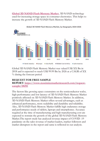
Introduction • NAND Flash is a rapidly changing technology and market. It promises to be very interesting as the process node approaches 10 nm. At this point, physical constraints will begin to limit the performance of the basic memory cell design. As a result, looking more than two years into the future becomes a purely speculative exercise and we limit our projections to 2016. • Contact us for more information: • http://www.techinsights.com/company/contact-us/ • 1-613-599-6500 Content for re-use only with TechInsights permission.
ITRS Technology Roadmap Source: ITRS Content for re-use only with TechInsights permission.
NAND Annual Technology Roadmaps Content for re-use only with TechInsights permission.
NAND Technology Quarterly Forecast Content for re-use only with TechInsights permission.
2013 NAND Production Source: http://en.chinaflashmarket.com/Uploads/file/2013%20NAND%20Flash%20market%20annual%20report.pdf Content for re-use only with TechInsights permission.
Micron Memory Roadmap Source: http://www.enterprisetech.com/2014/02/20/micron-pushes-memory-roadmap-several-routes/ Content for re-use only with TechInsights permission.
Micron 16 nm MLC NAND Our 16 nm NAND technology enables the industry’s smallest 128Gb MLC Flash memory device. The 16 nm node is not only the leading Flash process, but it is also the most advanced processing node for any sampling semiconductor device. Micron plans to make the transition from 2D NAND flash to 3D NAND flash when it's more cost effective. Because Micron already has a good scaling path for 2D NAND flash, it needs to add a lot of layers to 3D NAND flash before it makes economic sense to change over, so it is pursuing both formats in parallel. Source: http://www.micron.com/about/innovations/process-tech Source: http://www.theinquirer.net/inquirer/feature/2286446/micron-bets-on-3d-nand-flash-for-the-future-of-storage Content for re-use only with TechInsights permission.
Micron 3D NAND Cell Micron customers won't have to wait long for 3D flash memory CEO Mark Durcan tells CNET that the company will start providing samples of the advanced memory technology to customers in the first quarter of 2014. Source: http://www.cnet.com/news/micron-customers-wont-have-to-wait-long-for-3d-flash-memory/ Source: Akira Goda “Opportunities and Challenges of 3D NAND Scaling” International Symposium VLSI Technology, Systems, and Applications (VLSI-TSA), 2013 Content for re-use only with TechInsights permission.
Samsung NAND Flash Roadmap Source: http://www.anandtech.com/show/7237/samsungs-vnand-hitting-the-reset-button-on-nand-scaling Content for re-use only with TechInsights permission.
Samsung 3D V-NAND Samsung's three-dimensional V-NAND (Vertical NAND) flash memory is fabricated using an innovative vertical interconnect process technology to link the 24-layer 3D cell array based on Samsung's 3D Charge Trap Flash (CTF) structure. In Samsung's CTF-based NAND flash architecture, first developed in 2006, an electric charge is temporarily placed in a holding chamber of a non-conductive layer of flash composed of silicon nitride (SiN), instead of using a floating gate, to mitigate interference between neighbouring cells. By making this CTF layer three-dimensional, the reliability and processing speed of our V-NAND has been significantly improved. Furthermore, by applying both of these technologies, Samsung's 3D V-NAND is able to provide over twice the scaling of 20 nm-class planar NAND flash. Source: http://www.samsung.com/global/business/semiconductor/html/product/flash-solution/vnand/overview.html Content for re-use only with TechInsights permission.
Samsung 3D V-NAND Source: http://www.anandtech.com/show/7237/samsungs-vnand-hitting-the-reset-button-on-nand-scaling Content for re-use only with TechInsights permission.
Samsung 3D V-NAND Source: Ki-Tae Park et al. “Three-Dimensional 128Gb MLC Veritical NAND Flash-Memory with 24-WL Stacked Layers and 50MB/s High-Speed ProgrammingSolid-State Circuits Conference Digest of Technical Papers (ISSCC) 2014 pp334-335 Content for re-use only with TechInsights permission.
Sandisk NAND Memory Roadmap Source: http://www.flashmemorysummit.com/English/Collaterals/Proceedings/2013/20130813_Plenary_Shrivastava.pdf Content for re-use only with TechInsights permission.
Sandisk 2D NAND Memory ”One of our goals is to extend the life of 2D NAND technologies as far as possible because it reflects the huge investment that we have made in fabs and the technology, over the number of years,” said Shrivastava. “Of course, 3D NAND is extremely important and when it becomes cost-effective then it will move into production.” Sandisk plans to start producing its 3D NAND chips in 2016. “We are travelling in what we think is the lowest cost path in every technology generation, going from 19 nm to 1Y where we at the limit with lithography, and then we will scale to 1Z, which is our next-generation 2D NAND technology. We believe that this scaling path gives us the lowest cost structure in each of the nodes and in terms of cumulative investment.” Source: http://www.flashmemorysummit.com/English/Collaterals/Proceedings/2013/20130813_Plenary_Shrivastava.pdfRitu Shrivastava, Vice President Technology Development, at Sandisk Corporation Content for re-use only with TechInsights permission.
Sandisk BiCS 3D-NAND Source: http://www.flashmemorysummit.com/English/Collaterals/Proceedings/2013/20130813_Plenary_Shrivastava.pdf Content for re-use only with TechInsights permission.
SK-Hynix NAND Roadmap Source: 2013SK_hynix_en_1.pdf www.skhynix.com/en/sustainable/sustain/report.jsp Content for re-use only with TechInsights permission.
SK-Hynix 2D NAND Memory SK Hynix Inc. announced that it has started full-scale mass production of 16 nm 64 Gb (Gigabit) MLC (Multi Level Cell) NAND Flash, which uses the industry's thinnest process technology. (Nov.20 20013) We expect Hynix will develop 3D vertical fabrication technology by year-end or early next year and determine commercial production timing later. Given very low presence in the SSD market, unlike other NAND makers, Hynix’s priority in R&D and product development will be on enhancing competitive in house controller capability to set up a more sustainable product portfolio, according to the company. Source: http://www.techpowerup.com/194824/sk-hynix-started-full-scale-mass-production-of-16-nm-nand-flash.htm Source: Global Memory Sector Citi Research Equities 26 Sept 2013http://pg.jrj.com.cn/acc/Res/CN_RES/INDUS/2013/9/27/2b21dda8-af3a-4861-8b9e-69ad4e9efd5e.pdfl Content for re-use only with TechInsights permission.
SK-Hynix MLC NAND Product Offerings Source: SK-Hynix Content for re-use only with TechInsights permission.
SK-Hynix 3D V-NAND Source: http://thememoryguy.com/3d-nand-who-will-make-it-and-when/ Content for re-use only with TechInsights permission.
Glossary • BiCS- pipe-shaped Bit Cost Scalable flash. A 3D NAND cell being developed by Toshiba. • eMMC- Embedded Multimedia Card. A 1997 standard combining NAND Flash and Controller. • HKMG- High K Metal Gate. An advance technology designed to replace silicon dioxide at small process nodes. • ITRS- International Technology Roadmap for Semiconductors. • MLC- Multilevel Cell. A NAND memory cell that stores more than one bit of information. • TCAT- Terabit Array Transistor. A 3D NAND cell architecture. • TLC- Triple Level Cell. A NAND memory cell that stores three bits of information. Content for re-use only with TechInsights permission.