Electrical Properties for Metallic Nanowires
60 likes | 413 Views
Electrical Properties for Metallic Nanowires. Investigator: Carmen M. Lilley, Mechanical Engineering Prime Grant Support: NSF.

Electrical Properties for Metallic Nanowires
E N D
Presentation Transcript
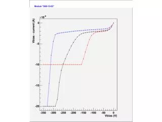
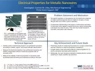
Electrical Properties for Metallic Nanowires Investigator: Carmen M. Lilley, Mechanical Engineering Prime Grant Support: NSF • Successful integration of nanosystems into microelectronics depends on stable material properties that are reliable for at least a 10 year lifecycle with over a trillion cycles of operation. • Fundamental understanding of the physics of deformation and failure in nanometer scale capped or layered structures, where surfaces play a dominant role, does not exist. Prior work has mostly focused on monolithic nanometer scale materials. FIG. 2: Electromigration of a Cu nanowire with the current stress of 4.2 mA (length = 2.04 µm, width = 90 nm, and thickness = 50nm): (a) 0 min, (b) 40 min, (c) 80 min, (d) 120 min, and (e) 137.5 min. FIG. 1: (a) Micrograph of a Ag nanowire under 4-probe I-V measurement, (b) STM scan of the cross-section from left-to-right, (c) line scan profile of cross-section from left-to-right (solid curve) and right-to-left (dashed curve). • Preliminary results on measuring the presence of surface contaminants and their influence on electrical properties completed [1]. • In depth study on size and surface effects on electromigration for Cu and Au nanowires have been performed [2-4] • Additionally, this work has been extended to studying electron surface scattering for single crystalline Ag nanowires. • Identify surface contaminants present in as-synthesized nanowires according to metallic, organic, and mixed-materials classifications. • Measure the electrical properties of as-synthesized nanowires and identify contamination effects on electrical properties with an accuracy of 5%. • Measure the stability of electrical properties of nanowires under accelerated electrical testing and classified according to structure. [1] C. M. Lilley, Q. J. Huang, Applied Physics Letters2006, 89, 203114. [2] Q. J. Huang, C. M. Lilley, M. Bode, R. Divan, Journal of Applied Physics2008, 104, 23709. [3] Q. Huang, C. M. Lilley, R. Divan, Nanotechnology2009, 20, 075706. [4] Q. Huang, C. M. Lilley, R. S. Divan, M. Bode, IEEE Transactions in Nanotechnology2008, 7, 688.]