Download
1 / 11
140 likes | 501 Views
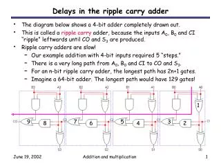
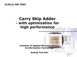
VLSI(2) SW 2005. Carry Skip Adder - with optimization for high performance. Institute of Applied Microelectronics & Information Technology Kwang Yoal Kim. A 0. B 0. A 1. B 1. A 2. B 2. A 3. B 3. FA. FA. FA. FA. C 0 =C in. C out =C 4. S 0. S 1. S 2. S 3.

E N D
VLSI(2) SW 2005 Carry Skip Adder - with optimization for high performance Institute of Applied Microelectronics & Information Technology Kwang Yoal Kim
A0 B0 A1 B1 A2 B2 A3 B3 FA FA FA FA C0=Cin Cout=C4 S0 S1 S2 S3 The Ripple Carry adder S = A B Ci = ABCi + ABCi+ ABCi Co = AB+ BCi+ ACi Ge= AB, De = AB, Prop = AB Co(G,P) = G+ PCi S(G,P) = P Ci
P0 G0 P1 G1 P2 G2 P3 G3 Co,0 Co,1 Co,2 FA FA FA FA Ci,o Co,3 “Block Propagate” BP = P0 P1 P2 P3 The Carry skip adder If (P0 & P1 & P2 & P3 = 1) then Co,3 = Ci,0 otherwise the block itself kills or generates the carry internally
BP P1 P2 P3 P0 Cout Cin G1 G2 G3 G0 BP Carry skip Implementation block carry-out carry-out BP block carry-in
4bit Block Carry skip adder bits 0 to 3 bits 4 to 7 bits 8 to 11 bits 12 to 15 Setup Setup Setup Setup Carry Propagation Carry Propagation Carry Propagation Carry Propagation Ci,0 Sum Sum Sum Sum Worst-case delay carry from bit 0 to bit 15 = carry generated in bit 0, ripples through bits 1, 2, and 3, skips the middle two groups (M is the group size in bits), ripples in the last group from bit 12 to bit 15 Tp = tsetup + M tcarry + (N/M - 2) tskip + (M-1) tcarry + tsum
Block size & time optimization • Assuming one stage of ripple (tcarry) has the same delay as one skip logic stage (tskip) and both are 1 TCSkA = 1 + M + (N/M-2) + (M-1) + 1 tsetupripplein skips ripple in tsum first block last block = 2M + (N/M) - 1 • So the optimal block size, M, is dTCSkA/dM = 0 (N/2) = Mopt • And the optimal time is Optimal TCSkA = 2((2N)) - 1
Cout Cin Cout Cin skip level 1 skip level 2 logic optimization • Variable block sizes - What if block sizes are of the same size? • Multiple levels of skip logic - Can we skip over several blocks at once?
28 0 24 20 4 16 12 8 5 1 9 13 21 29 25 17 18 10 22 26 6 14 30 2 11 31 7 27 19 23 15 3 Setup Setup Setup Setup Setup Setup Setup Setup Cin Sum Sum Sum Sum Sum Sum Sum Sum Variable block sizes 1. • Fixed block sizes carry skip adder If all the skip blocks are of the same size, the latter blocks will finish switching quickly and then sit idle for a while waiting for the carry signal to pass through all the bypass multiplexers. (Example. 32-bit carry-skip adder) The carry-out for bits 4-7 will be ready at the same time as the carry-out for bits 0-3. This second block will wait while the first multiplexer does its job.
Setup Setup Setup Setup Setup Setup 0 1 2 3 4 5 6 7 8 9 10 11 12 13 14 15 16 17 18 19 20 21 22 23 24 25 26 27 28 29 30 31 Cin Sum Sum Sum Sum Sum Sum Variable block sizes 2. • Variable block sizes carry skip adder To speed up the circuit, we could vary the size of the skip block. Intuitively, we should then be able to reduce the size of the first skip block and make each subsequent block increasingly larger. Because the critical path includes the last skip block, we must also start to taper down the size of each block as we approach the end.
Multi-level Carry skip adder • 2 skip level carry skip adder A two level carry skip adder and the signal controlling this second skip level logic is derived as the logical AND of the first level skip signals. A carry that needs 3 time units to skip these three blocks in a single level skip adder can do the same work in a single time unit. Cout Cin skip level 1 3 Delays skip level 2 1 Delays AND of the first level skip signals (BP’s)
Carry skip adder • Faster and Simple - O(N) delay (ripple carry adder O(N) delay) - simple and regular layout - optimization can be considered • Still linear fashion and extra overhead - linear fashion delay (ripple carry is faster with small bit) - everhead of extra skip multiplexer • Simplifying assumption of optimization - skip and ripple delays are equal - ripple delay is linearly proportional to block width - the exact optimal configuration is technology dependent