Download
1 / 42
420 likes | 654 Views
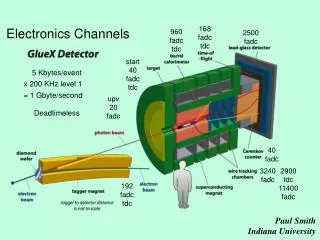
IPAS SPring-8 FADC Project. 章文箴 蘇大順 04/26/2002. Super Photon Ring 8 GeV (SPring-8). Harima Science Garden City. Laser Electron Photon. LEPS Detector Configuration. TPC inside LEPS Detectors. Time Projection Chamber. Working Principles of Time Projection Chamber.

E N D
IPAS SPring-8 FADC Project 章文箴 蘇大順 04/26/2002
Super Photon Ring 8 GeV (SPring-8) Harima Science Garden City
Working Principles of Time Projection Chamber • Passage of charged particles through the gas generates ionization electrons. • Electrons drift towards the readout plane along the imposed E x B drifting fields. • At the end of readout plane, an avalanche (amplification) will happen upon the arrival of electrons by the proportional sense wires and an induced image charge on the corresponding cathode pads. • The pads are connected with a read-out electronics which provides low-noise and high resolution analogue information as well as the drift time associated with the signal.
Electric Field Configuration Grid Wire Sense Wire Field Wires Cathod
TPC Mechanical Specification • Inner radius: < 1.25 cm. • Outer radius: < 30 cm. • Read out channels: 95 sensing wires, 1000 pads. • Pad size:inner 8mm*8mm, outer 8mm*13mm. • Distance between sensing wires and pads: 4mm. • Separation of sensing wire: 4mm. • Cathode readout. • Maximum drift distance : about 70 cm. • Maximum drift time: about 14 sec with drift velocity = 5.1 cm/sec.
Requirement of TPC Electronics • Good energy resolution: measuring dE/dx from the charge readout of either wires or pads for the particle identification for K/p separation at low momentum. • Requirement of spatial resolution: • x,y < 300 m. • z < 1 mm. • Position information: • x(t),y(t): x from fired sense wires; y from interpolation of signals on pads(t). • z(t) from time bin of FADC time slice. • Timing information: fitting of pulse peak in FADC. • On-board zero-suppression to ensure fast data transfer and short system dead time.
Digitizer in TPC Electronic: FADC • Large data size: • High sampling rate: 40 MHz = 25 nsec. • Read-out bit (Nbit): 10 bits. • # of Time bins per event: ~600 time bins. (Max drift time/clock = 14 sec/25 nsec = 560 bins.) • 1000 channels. • Trigger latency: 1 sec . • On-board zero-suppression. • Need of a large buffer size to store 4-5 events on board for one single VME readout.(16*600*5=48K per channel, w/o a zero suppression factor.) • High channel density.
SPring-8 FADC Module • Use TEXONO FADC and IHEP BES version as the starting point. • 40 MHz; 10-bit FADC: input 0-2 V range. • Shift register inside FPGA: length = trigger latency (1 s). • On-board FPGA for threshold suppression. • Buffer FIFO: dual port memory. • CPLD: controlling VME actions. • Free clock running. • VME 9U; 32 channels/module; 8 attached cards/module; 4 channel/card.
Main Electronic Components • Receiver: MAXIM, MAX4145ESD. • OPA: Analog Device, AD8138ARSO-8. • FADC: Analog Device, AD9203ARVRU-28. • FPGA: Xilinx, XC2S150-6FG456. • FIFO: TI, SN74V245.
SPring-8 FADC Module(4 channels, 10 bits, 40 MHz) FIFO FADC OPA FPGA
Mixed signal AD Converter Adapter Board • 40 MHz sampling rate. • 10 bits resolution with 2Vp-p dynamic range. • Clock distribution with Phase Lock Loop circuit. • On Board digital signal delay and • Real-Time ZERO-Suppression. • High capacity First In First Out Memory. • Easy to use with high density connector.
FADC Mother Board Driver CPLD Clock Driver VME Connector
VMEBus slave controller, with high performance BLTransfer Mode. FPGA, digital signal control chip. First In First Out memory. Differential AD Converter (40 MHz) 16 channels differential signal input connector. 32 Channels, high sampling rate Flash AD converter. Spring-8 2002/03
10 Clock Trigger Differential Signal from MAMP x 8 Four Channels Receiver & Driver 10 CH 1 FADC Download PROM Receiver & Driver CH 2 FADC Processing FPGA VA[8..15] VD[0..31] Receiver & Driver 10 CH 3 FADC Download PROM Read Receiver & Driver 10 RST CH 4 FADC Write Flag Flag 4 Hit Flag FIFO VD[0..31] VD1 x 8 JTAG VD[0..11] 12 Trigger Counter Trigger FIFO VD[0..11] Reset Read Flag Write_in Read_out Write Delay VME Control Read Trigger FIFO VA[8..23] Clear Trigger FIFO VA1 Check Trigger Number VC AS,D0,D1,AM[0..5],Write,DTACK, et. al. VME_Reset 8 Global FPGA 8 bits DIP Switch
10 32 bits FIFO L=(Trigger Latency + 1) 10 bits Data Shift Register 10 Clock Write Enable 10 Write Read Comparator Flag Q S 10 Threshold R VD[0…15] VD2 Write Flag VA[8…15] VA2 Read Clock Counter & Control Count Over_Threshold Trigger Enable Comp_Control Clock Clock Write_header&trailer Rst Write_Data Reset Write_Flag Disable Clear Fig. 2 Block Diagram of Processing FPGA
CS: Checksum bit Data Format Lowest Bit ND: Not defined. Header 1 Header 2 ADC Time Trailer
CSR Format Lowest Bit VME address: 0x010000 Reset Sampling Count: default value 1020.
FADC VME Action List (A24/D16) • 0x0i0000: address to write, bit 9 for resetting FIFO and set ready, bit 10 for resetting suppression threshold and bit 11 for setting the sample count of the FADC i. (Address modifier: 0x3D). • 0x0i0100: address to read the merged 32 FIFOs’ content in BLT mode for FADC i. (Address modifier: 0x3B, 0x3F). • 0x0i0101: address to read the BLT reading cycle for FADC i. (Address modifier: 0x3B, 0x3F). • 0x0i0000+j*0x000100: address to read the single FIFO content in AO mode for channel j. (Address modifier: 0x3D) • 0x0i0000+j*0x000100: address to write for setting the zero-suppression threshold for channel j. (Address modifier: 0x3D)
The Control Flow of FADC For each channel DAQ Start Trigger , Conversion Master Yes NIM < 5 events Preamplifier Module VME CPU No Trigger Count *Veto Send IRQ to VME CPU Trigger signal DAQ READ FIFO CPLD FADC Trigger Clock 100MHz DAQ send Reset FADC Module Trigger FADC clear BUSY FADC Reset Clear trigger Veto Busy Slave
Observation Window of Signals Signal Shift Register Length ( max 100*25ns = 2.5 s) Trigger Conversion Strobe Sampling Counts ( max 1024*25ns=25s)
LeCroy222 TEXONO MAMP Full scale width 10 1.0 100 L VT 100 1.0 10 10 1.0 LATCH H VT LTDS1 Voltage Reference START BUSY STOP Rst OR NIM LTD0 DEL BLANK TTL Strb Full scale width 10 1.0 SCLK 100 100 Clock Generator 1.0 HTD0 10 10 1.0 LATCH Evnt START BUSY STOP NIM OR DEL BLANK TTL INT FBSY CLK Reset READ Trigger Busy SPring-8 32-channel FADC +5V -5.2V +12V -12V DAQ Trigger Logic
ROOT Offline Event Display for 2 SPring-8 FADC (64 channels) Module 1 Module 2
Events • 02/09/2001: Prof. Imai and Ahn visited AS. Collaborating plan was discussed and finalized. • 03/31/2001: Wen-Chen and Henry visited IHEP, Beijing and explored the R&D plan in IHEP. • 05/31/2001: IHEP was not able to perform the R&D plan. • 08/01/2001: Da-Shun visited IHEP for 3 weeks to learn the conceptual design. • 02/01/2002: Prototype 1 boards made. • 02/28/2002: Wen-Chen and Da-Shun tested prototype-1 boards with TPC at SPring-8. • 04/25/2002: Finished up 64 channels of prototype-1 and deliver them to SPring-8.
Plan • 04/30/2002: Issue out prototype-2 (quasi-final) fabrication order. • 05/21/2002: Deliver prototype-2 to SPring-8. • 06/01/2002: System test with a complete electronic chain (Pre-amp, shaper, and FADC) with TPC and Solenoid magnet. • 06/15/2002: Issue out final production fabrication order (1440 channels). • 07/01/2002: Send production boards for stuffing. • 07/15/2002 – 07/31/2002: Test production boards. • 08/01/2002 – 08/31/2002: Delivery of production board, installation, system test and DAQ. • 09/15/2002: Commission Run with photon beam.
Remarks • Many valuable experiences learned: board design, firmware, modification of TEXONO DAQ, coordinating people, etc. • A good starting point for a continuing “rooting” process of experimental technique at IPAS. • Thanks to many people: Henry, P.K., A.C., K.C., Tracy, IHEP group….