Download

1 / 17
170 likes | 363 Views
Prototype Test of SPring-8 FADC Module. Da-Shung Su Wen-Chen Chang 02/07/2002. Lab. Status of Prototype Test. 4-channel FADC card: Conversion of analog input into digital output in differential OPA and FADC. Functionality of shift register in FPGA.

E N D
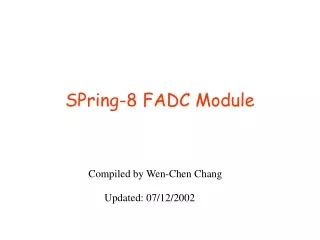
Prototype Test of SPring-8 FADC Module Da-Shung Su Wen-Chen Chang 02/07/2002
Status of Prototype Test • 4-channel FADC card: • Conversion of analog input into digital output in differential OPA and FADC. • Functionality of shift register in FPGA. • Functionality of data writing into FIFO from FPGA. • FADC mother board: • Functionality of single action of VME “read” and “write” by NI-VXI software.
To be finished before TPC on-site test 03/03-03/15 • Zero suppression and fine timing tuning in FPGA. • Implement VME BLT read action into CPLD. • Stuffing 16 4-channel FADC cards and 2 FADC mother boards. • Overall system test using TEXONO DAQ for reading calibration pulse. Exercising the coordination with trigger and DAQ system. • Check the validity of offline reconstruction of data.
SPring-8 FADC Module(4 channels, 10 bits, 40 MHz) FIFO FADC OPA FPGA
4-channel FADC card OPA FADC FPGA FIFO
FADC Mother Board Driver CPLD Clock Driver VME Connector
FADC Mother Board CPLD
Left: FADC inputRight: FADC readout Clock: 10 MHz
Digital Delay in FPGA:functioning of Shift Register 8 micro-sec (80 time bins) delay
Logic Analyzer: FPGA->FIFO Time bin counter Header of event Trailer of event ADC Write of event Time Write of event
CS: CheckSum bit Data Format Lowest Bit ND: Not defined. Header ADC Time Trailer
FADC VME Action List (A24/D16) • 0x0i0000: address to write 0x0100 for resetting the FADC i. (Address modifier: 0x3D). • 0x0i0001: address to write for setting the sampling count of FADC i. (Address modifier: 0x3D). • 0x0i0100: address to read the merged 32 FIFOs’ content in BLT mode for FADC i. (Address modifier: 0x3B, 0x3F). • 0x0i0101: address to read the BLT reading cycle for FADC i. (Address modifier: 0x3B, 0x3F). • 0x0i0000+j*0x000100: address to read the single FIFO content in AO mode for channel j. (Address modifier: 0x3D) • 0x0i0000+j*0x000102: address to write for setting the zero-suppression threshold for channel j. (Address modifier: 0x3D)
The Control Flow of FADC For each channel Start Measurement Master Yes NIM < 5 events Preamplifier Module VME CPU No Trigger Count *Veto Send IRQ to VME CPU Trigger signal CPU start read action CPLD FADC Trigger Clock 100MHz CPU send reset FADC Module Trigger FADC set ready FADC Reset Clear trigger Veto Clear Slave
Things to finish up during SPring-8 visit • Complete one full 32-channel FADC module. • Finalize and implement the VME action list. • Determine and implement the default values for shift register length and sampling count. • Implement the functions of “reset” and “ready” on the front-panel inputs and the definition of LED light. • Fix up the gain range and signal coupling on the analog input. • DAQ.
Things to do after Spring-8 visit • Finish up another 32-channel FADC module and ship it for use by the end of March. • Get the feedback and finalize the layout and part lists for FADC modules. • Issue the purchase orders of electronic parts and board fabrication by 04/15.