Optical methods for semiconductor characterization
Optical methods for semiconductor characterization. Guillaume von Gastrow. I. Introduction. Optical measurements: contactless methods, no preparation Three categories. Photometric. Measurement of the intensity e.g. optical microscope, reflection measurements . Interference.

Optical methods for semiconductor characterization
E N D
Presentation Transcript
Optical methods for semiconductor characterization Guillaume vonGastrow
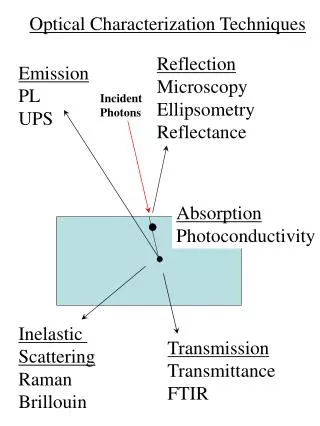
I. Introduction Optical measurements: contactless methods, no preparation Three categories Photometric Measurement of the intensity e.g. optical microscope, reflection measurements Interference Measurement of the phase e.g. interferometric spectroscopy Measurement of the electric field direction e.g. ellipsometry, Raman spectroscopy Polarization
Parameters measured by optical methods • Physical characteristics • Optical constants • Thickness • Linewidth • Crystallographic structure • Defects and impurities • deep/shallow level impurities • particles e.g. photoluminescence, elastic light scattering e.g. transmittance spectroscopy, Raman spectroscopy, ellipsometry Measured characteristics e.g. optical microscope, interference contrast microscope, ellipsometry • Sample aspect • Thickness • Shape • Cross section • Surface aspect
Outline I- Observation of the sample – optical microscopy a. Fundamental notions b. Techniques II- Measurement of the physical characteristics III- Detection of defects and impurities
Optics notions • Focal point: for an optical system, point where the rays parallel to the optical axis converge (or seem to converge) Source: http://www.bradleypatten.co.nz • Focal plane: plane perpendicular to the optical axis • and containing the focal point
Interference phenomenon Caused by interaction between several coherent light sources that have the same amplitude but a phase difference source: http://gilbert.gastebois.pagesperso-orange.fr • Optical path difference • Constructive interference if • Destructive interference if with m natural integer
I- Sample observation with optical microscopya. Fundamental notions • Microscope performance is limited by interferences • The angular position of the first minimum is given by • : demi-angle of the cone • D: aperture diameter • Rayleigh principle: two objects can be distinguished if the central maximum of one coincides with the first minimum of the other • Maximum resolution achievable
I- Sample observation with optical microscopy a. Fundamental notions Example: for a good numerical aperture i.e. NA=1, and =500 nm the minimum separation is s = 0,305 m
I- Sample observation with optical microscopya. Main techniques 1. Optical microscope Focus when the resulting image is at infinity (schema) Source: http://ressources.univ-lemans.fr
I- Sample observation with optical microscopy a. Main techniques 1. Optical microscope Contrast is reduced by: • Dirty lenses (of course!) • Too powerful light Illumination can be controlled by the diaphragm aperture
I- Sample observation with optical microscopya. Main techniques 2. Confocal microscope Principle: 3D picture of an object thanks to different focalizations. One pixel at a time, light outside of the focal plan is eliminated. Better contrast Resolution: Applications: scanning trough the sample (e.g. different heights in integrated circuits)
I- Sample observation with optical microscopya. Main techniques 2. Confocal microscope Examples of confocal microscope pictures (Lasertech corporation)
I- Sample observation with optical microscopya. Main techniques 3. Interferometric spectroscopy • Application • Determine vertical and horizontal features of a sample. • Principle (phase-shift interferometry) • For a monochromatic wave intensity after interference of two waves of intensity I0: h(x,y) is the comparison of the sample height with a reference mirror
II- Physical parameters measurements • Optical constants (refractive index, absorption constant) • Layer thickness • Linewidth • Crystallographic structure
II- Physical parameters measurements 1. Ellipsometry Measures the change of polarization of light reflected from a surface. Source: http://jawoollam.com
II- Physical parameters measurements 1. Ellipsometry The characteristics of the sample are calculated from the amplitude and phase change and of the electric field component.
II- Physical parameters measurements 1. Ellipsometry • Principle: Case of rotating analyzer ellipsometry Light intensity at the detector: • Fit of the curve for and • Calculate and • Calculate n and k • Applications • Measurement of optical constants • Film thickness
II- Physical parameters measurements 1. Ellipsometry
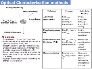
II- Physical parameters measurements 2. Raman spectroscopy • Principle • Activation of the vibration modes of a crystal by polarized light • The wavelength of the reemitted photons shifts • Analysis of the polarization changes of the reflected light after FTIR (Fourier Transform Infrared Spectroscopy) • Applications • - phase transition measurements • - crystallinity tests (structure, orientation) • stress measurements • also impurities detection Examples of vibration modes (perovskite ABO3)
II- Physical parameters measurements 2. Raman spectroscopy Example of a Raman spectrum after FTIR: intensity I in function of the polarization angle and the frequency f (perovskite, DyScO3)
II- Physical parameters measurements 2. Raman spectroscopy
II- Defects and impurities • Semiconductorimpurities (deep and shallowlevel) • surface particles 1/3 of the smallest circuit dimension (eggatethickness) isalreadydetrimental
II- Defects and impurities 1. Photoluminescence • Applications Used for shallow-level impurities detection + deep-level if radiative recombination is possible • Principle Measurement of the internal efficiency, related to radiative electron/hole pairs recombination Fig. : Different types of recombination Band-to-band Free exciton (c) Bound exciton (d) Free e/hole pair (e) Acceptor donor
II- Defects and impurities 1. Photoluminescence • Bound exciton recombination dominates over free exciton recombination for less pure material. PL of a GaN structure (http://www.ioffe.rssi.ru)
II- Defects and impurities 2. Elastic light scattering • Principle Detection of the light scattering by surface particles in all directions. The detectors are placed at various locations. The scattered light is proportional to the optical scattering cross-section (for D « ): D: particle diameter : laser wavelength K: relative dielectric constant of the particle Particle density detected by scanning the laser across the sample
II- Defects and impurities 2. Elastic light scattering
Conclusion • Main advantages of optical characterizations: • - Often easy to perform • Contactless • Non-destructive • Even basic methods have a lot of additional features