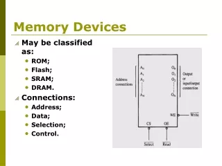
Download
1 / 17
240 likes | 601 Views
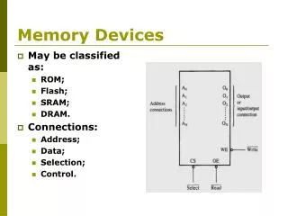
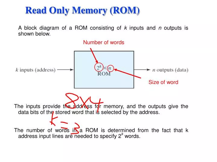
Read Only Memory (ROM). A block diagram of a ROM consisting of k inputs and n outputs is shown below. The inputs provide the address for memory, and the outputs give the data bits of the stored word that is selected by the address.

E N D
Read Only Memory (ROM) • A block diagram of a ROM consisting of k inputs and n outputs is shown below. • The inputs provide the address for memory, and the outputs give the data bits of the stored word that is selected by the address. • The number of words in a ROM is determined from the fact that k address input lines are needed to specify 2k words. Number of words Size of word
Read Only Memory (ROM) Memory Size: 102416
Read Only Memory (ROM) Draw a 32 8 ROM. The unit consists of 32 words of 8 bits each.
Read Only Memory (ROM) Inputs outputs . I4 I3 I2 I1 I0 A7A6A5A4A3A2A1A0 1 0 1 1 0 1 1 0 0 0 0 0 0
Read Only Memory (ROM) Example 7.1: Design a combinational circuit using a ROM. The circuit accepts a three-bit number and outputs a binary number equal to the square of the input number. (minimize the ROM if possible)
Read Only Memory (ROM) Example 7.1: Design a combinational circuit using a ROM. The circuit accepts a three-bit number and outputs a binary number equal to the square of the input number. We need a ROM with a size = 8 4
FPGAs are programmable digital logic chips. What that means is that you can program them to do almost any digital function.Here's the general workflow when working with FPGAs: • You use a computer to describe a "logic function" that you want. You might draw a schematic, or create a text file describing the function, doesn't matter. • You compile the "logic function" on your computer, using a software provided by the FPGA vendor. That creates a binary file that can be downloaded into the FPGA. • You connect a cable from your computer to the FPGA, and download the binary file to the FPGA. • That's it! Your FPGA behaves according to your "logic function". • Keep in mind that • You can download FPGAs as many time as you want - no limit - with different functionalities every time if you want. If you make a mistake in your design, just fix your "logic function", re-compile and re-download it. No PCB, solder or component to change. • The designs can run much faster than if you were to design a board with discrete components, since everything runs within the FPGA, on its silicon die. • FPGAs lose their functionality when the power goes away (like RAM in a computer that loses its content). You have to re-download them when power goes back up to restore the functionality.
Programmable Logic Array (PLA) F1=AB\+AC+A\BC\ F2=(AC+BC)\
Programmable Logic Array (PLA) • Example 7.2 :Implement the following two Boolean functions with a PLA: • F1(A, B, C)= (0,1,2,4) • F2(A, B, C) = (0,5,6,7) F1 F2 F1= A\B\+A\C\+B\C\ F2= AB+AC+A\B\C\ F1= (AB+AC+BC)\ F2= (A\B+A\C+AB\C\)\
Programmable Logic Array F1= (AB+AC+BC)\ F2= AB+AC+A\B\C\