Download
1 / 40
440 likes | 838 Views
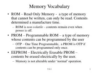
Memory Vocabulary. ROM – Read Only Memory - a type of memory that cannot be written, can only be read. Contents determined a manufacture time. ROM is non-volatile – contents remain even when power is off. PROM – Programmable ROM – a type of memory whose contents can be programmed by the user

E N D
Memory Vocabulary • ROM – Read Only Memory - a type of memory that cannot be written, can only be read. Contents determined a manufacture time. • ROM is non-volatile – contents remain even when power is off. • PROM – Programmable ROM – a type of memory whose contents can be programmed by the user • OTP – One Time Programmable, a PROM is OTP if contents can be programmed only once. • EEPROM – Electrically Erasable PROM – contents be erased electrically by the user. • Memory is not alterable under ‘normal’ operation. V 0.1
Memory Vocabulary • RAM – Random Access Memory – memory that can be both read and written during normal operation. • Contents are non-volatile, will be lost on power off. • SRAM – static RAM – has the following characteristics: • Read, Write operations take equal amounts of time • Access to any ‘random’ location takes same amount of time. • Fastest access time of memory types. • Basic memory cell is a latch, takes 6 transistors per memory bit. V 0.1
Static Random Access Memory (SRAM) • The serial EEPROM had low pin count because of serial I2C interface • Speed was sacrificed • Random access read took 5 bytes (3 bytes to set address, 2 bytes for read). Total of 45 bit times (5 * 9), @400 KHz this took 2.5 s * 45 = 112.5 s! • Write speed was slow because non-volatile memory (page write took about 6.5 ms for 64 bytes, or about 101 s/byte. • An SRAM (Static Random Access Memory) has: • equal read/write times, measured in nanoseconds • volatile (contents not maintained when power removed) • equal cycle time, access time • typically has a parallel interface V 0.1
Typical SRAM Control Lines K x N Address[log2(K)-1:0] Data[N-1:0] MEM CS Data bus is bidirectional OE W Chip Select – must be asserted before Memory will respond to read or write operation. If negated, data bus is high impedance. OE – Asserted for read operation, Memory will drive data lines. W – Asserted for a write operation (Memory inputs data from data pins, processor writes to memory). V 0.1
Internal Architecture Bit Line Bias Row Address Cell MemoryOrganization Row Decode Word lines(1 per row) Column Address Sense Amps Bit lines(2 per column) Column Decode Data lines V 0.1
Static Ram Cell Wordline B (bitline) BB (bitline_bar) V 0.1
Cypress 8K x 8 SRAM Multiple Chip Enables – more flexibility Data bus is bi-directional (8 I/O lines). Note: a more precise name for this memory is Asynchronous SRAM. It has no clock input, any change on address inputs accesses a new location. V 0.1
Read Cycle Cycle Time – how fast can I start another operation? Access Time – how fast is data ready?For SRAMs, Cycle Time = Access Time, this is a feature of SRAMs. V 0.1
Write Cycle V 0.1
Write Timings Notice that Write Cycle = Read Cycle. All volatile RAM types have this feature. V 0.1
‘#’ means low true PIC To SRAM PIC 8Kx8 A[7:0] RA[7:0] A[12:8] RB[4:0] IO[7:0] RC[7:0] Vdd CE2 CE1# OE# RD0 WE# RD1 To read: Address on RA, RB. RC port is all inputs; RD0 = ‘0’, RD1 = ‘1’. To write: Address on RA, RB. RC port is all outputs; RD0 = ‘1’, RD1 = 0. V 0.1
RAM1 8Kx8 Expanding Memory A[7:0] RA[7:0] A[12:8] RB[4:0] IO[7:0] RC[7:0] CE2 RB5 CE1# OE# RD0 PIC WE# RD1 RAM0 8Kx8 RAM1 accessed when RB5 = 1 A[7:0] A[12:8] IO[7:0] CE1# RAM0 accessed when RB5 = 0 CE2 OE# WE# V 0.1
RAM0 RAM1 More Memory 13 A[12:0] RB[4:0], RA[7:0] A[12:0] 8 IO[7:0] RC[7:0] IO[7:0] OE# RD0 OE# RD1 WE# WE# PIC CE1# CE1# RB[6:5] 2-to-4 decoder RAM2 RAM3 RB[6:5]=00 A[12:0] 2 A[12:0] 0 RB[6:5]=01 IO[7:0] 1 IO[7:0] RB[6:5]=10 OE# OE# 2 WE# RB[6:5]=11 WE# 3 CE1# CE1# chip select decoding V 0.1
Memory Map Total memory = 4 * 8K = 32 K ( 25 * 210), 15 address lines Selects chip Selects location within chip RB[6:5] RB[4:0],RA[7:0] 1 1 1 1 1 0 0 0 0 0 0 0 0 0 0 4 3 2 1 0 9 8 7 6 5 4 3 2 1 0 0 0 0 0 0 0 0 0 0 0 0 0 0 0 00 0 1 1 1 1 1 1 1 1 1 1 1 1 1 0x0000 low RAM00x1FFF high 0 1 0 0 0 0 0 0 0 0 0 0 0 0 00 1 1 1 1 1 1 1 1 1 1 1 1 1 1 0x2000 low RAM10x3FFF high 1 0 0 0 0 0 0 0 0 0 0 0 0 0 01 0 1 1 1 1 1 1 1 1 1 1 1 1 1 0x4000 low RAM20x5FFF high 1 1 0 0 0 0 0 0 0 0 0 0 0 0 01 1 1 1 1 1 1 1 1 1 1 1 1 1 1 0x6000 low RAM30x7FFF high V 0.1
Other SRAM Types • SSRAM - Synchronous SRAM • Has a clock input • Address, data lines latched on clock edge • Can perform burst cycles • What is a burst cycle? • After first data value is output based upon address, data values in successive locations are output without needing to change address bus • Internal counter used for address value V 0.1
Synchronous SRAM (SSRAM) Note clock lines to SRAM. A DDR (Double Data Rate) SSRAM means that data is clocked on both clock edges. V 0.1
SSRAM Normal Cycle vs Burst Cycle Address ready, 1st data ready in 2 clocks, successive locations ready in successive clocks. This burst cycle is a 2-1-1-1 cycle. Diagram shows burst suspended for 1 clock between 3rd & 4th clock. Normal 2-1-1-1 burst takes 5 clocks. Address ready,Data ready in clocks. V 0.1
Why Burst Cycles? • Burst Cycles more efficient at block memory transfers (memory location is successive locations) • Normal cycle would take 8 clocks to transfer data from 4 locations. • 2-1-1-1 burst takes only 5 clocks. • Why do we want to transfer blocks of memory efficiently? • For cache fill operations. • So what is a cache? V 0.1
A Cache System 1st level cache CPU Single chip(die) Memory (SRAM) 2nd level cache Processor ModuleCasing Memory (SSRAM) 3rd level cache Memory (SSRAM) Motherboard Main Memory (DRAM) V 0.1
What is a Cache? • The “closer” a memory is to a CPU, the faster the data transfer between CPU and Memory. • Can’t get any closer than on the same chip as the CPU! • For high performance microprocessors, need LOTS of memory • Don’t have enough room to put all memory on same chip as CPU • Put some memory on same die as CPU, will not be able to hold all needed data/programs but will hold most frequently used data/programs • Will need to swap out some data if we don’t find what we need in the cache (a miss!). V 0.1
Memory Hierarchy Access/Speed Cost/Bit The further away, the slower the access time, the higher the capacity (density). Registers The further away, the cheaper per bit. Cache Main Memory Fixed Disk Tape Floppy Zip CD-ROM CD-RWR Capacity V 0.1
L1 instr. cache Intel 3rd Generation IA-64 (executes new 64-bit instructions) 0.13 IA-32 CPU (pentium, for compatibility) L2 cache cache and memory account for about 70% of the die. L3 cache V 0.1
Main Memory and DRAM • For main memory, we need a memory whose primary characteristics are: • Dense (lots o’ bits!!!) • Cheap (cause we don’t want to spend too much for our lots o’ bits!) • Good at block transfers, can be rotten at random accesses. • How do we achieve density? (lots o’ bits?) • Less transistors per bit! • Dynamic RAM (DRAM) - one transistor + capacitor per bit!!!!! V 0.1
DRAM Memory Cell Word line Turn this transistor on to access data Cs Memory value stored on capacitor ( a very small capacitor...) Bit line Data value appears on bit line V 0.1
DRAM Characteristics • Very dense (high capacity). Cheap per bit. • Slow for Random Access (access to any location) • Cycle time >> access time, Read Cycle time = Write cycle time. • Has special access modes to speed block transfers • Important since transfers to DRAM in modern computer system is always block-oriented for cache fills. • Only has half the address pins that you would expect • 1M x 8 DRAM has only 10 address pins instead of 20 • Reduces package size, can pack more DRAM chips per unit area. Address values multiplexed between row/column addresses V 0.1
A 1M x 16 DRAM (Micron Tech.) A0-A9 - 10 address pins DQ1-DQ16 – 16 data pins RAS# - row address strobe – asserted when address pins contain row address. CASL#, CASH# - column address strobe – asserted when address pins contain row address. Both need to be asserted for 16 bit transfers, only one for either high or low byte transfers. V 0.1
Address Muxing Assume a 16-bit data wide bus (D0-D15), and 20 address lines A20-A1 (no A0 pin since 16 bit-wide data bus). How are addresses split between Row, Column? A20-A11 A10-A1 Varies the fastest. Row Address Column Address A9-A0 CPU A20-A1 DRAMcontroller DRAM RAS# Chip select CASL# Decode CASH# V 0.1
DRAM Controllers • External logic called a DRAM controller needed to interface to DRAMs. • DRAM interfacing more complex than SRAM • Provides muxing of Address lines • Assertion of RAS, CAS lines • Also keeps DRAM contents refreshed • Capacitors tend to leak. Memory contents needs to continually accessed in order to keep contents valid. • Special ‘refresh’ cycles are supported by DRAMs to support refreshing all of bits in a row with one cycle • DRAM controller responsible for running refresh cycles. V 0.1
RAS asserted first CAS asserted next V 0.1
Block transfer. Access different bits on same row, change column address. V 0.1
Timing Values • Random access – Trc = 104ns, Trac = 50 ns (access time from row address strobe assertion) • Block Mode • Access time to data on row: 50 ns • To column locations on same row : 25 ns • Block transfer much more efficient than random access. V 0.1
DRAM Chip Generations • Each time a new DRAM Chip generation is released, capacity goes up by 4x • 16K x 1 (late 70’s), 64K x 1, 256K x 1, 1M x 1, 4M x 1, 16M x1, 64M x 1, 256M x 1 (current), 1G x 1 (samples available), 4G x 1 (in labs) • Why? because of muxed addresses, 1 address pin is actually two address bits. Two address bits give 4X more locations. V 0.1
DRAM Modules: SIMMs and DIMMs • Mount Memory Device Packages on Circuit Boards to Conserve Space • 30-Pin SIMM – First – Single Byte Access • Used in “Pairs” Since in x86 1 Word=16 bits • 72-Pin SIMM – Four Byte Access • Need Pairs for Pentium+ Since 64 bit Data Bus • 168-pin DIMM – Eight Byte Access • SIMM – Single In-Line Memory Module • DIMM – Dual In-Line Memory Module V 0.1
DRAM Modules SIMM – Single In-line Memory Module -- 72 pins Capacity varies Picture shows 8M x 32 (32 MByte) SIMMs/DIMMs invented to get denser packaging for DRAMs on motherboards. V 0.1
Memory Device Specification • “Dimension” of Storage Cell Array • 8 Mb – Refers to Eight Mega-bits (not Mega-Bytes!) • 8 Mb (lower case ‘b’ !!) • =(8)(1024)(1024)bits • =(1)(1024)(1024)Bytes • =1MB (upper case ‘B’!!) • Single 16Mb Device can be Arranged as: • 16M1 bits • 4M 4 nybbles • 2M 8 bytes • 1M 16 (words in the case of x86) • Many Devices are Typically “byte-wide” Devices • N8 V 0.1
DRAM Variations • SDRAM – Synchronous DRAM – has clock, supports burst transfers • DDR-SDRAM - Double Data Rate SDRAM • Data transferred on EACH clock edge • Double the data rate of SDRAM • RDRAM – Rambus DRAM • Will discuss this in more detail later • High speed signaling interface to support very fast data transfers • Very high latency (long access time to first location), but very fast at transferring successive locations – claim is better at block mode transfers than SDRAM/DDR-SDRAM. V 0.1
Dual Port Memories Address Address Dual Port Memory(SRAM, SSRAM) CPU CPU Data Data Control Control Support simulatenous access via two ports (left/right sides). Support simultaneous read accesses to different locations or same locations.Suports simultaneous write accesses to different locations Simultaneous write access to same location is not supported.One obvious application is multiple-processor systems, but useful in many other situations. V 0.1
Flash RAM • SRAM-like interface, density of SRAM • Non-volatile (retains contents when power is off) • Read Cycle time same as SRAM (10’s of nanoseconds) • Write Cycle >> Read Cycle • write times in microseconds • Can write individual locations or blocks of locations • Applications include smart cards (credit cards, medical history cards, etc) • Intel is market leader, has a Flash RAM cell that stores 2-bits per cell (can sense 4 different volage levels from cell). V 0.1
What do you have to know? • Differences between SRAM, DRAM in terms of density, speed, functionality • Pin functions of a SRAM • Memory decoding for SRAM via PIC example • Definitions of access time, cycle time for SRAM • Difference between Synchronous SRAM, Asynchronous SRAM • Dual Port, Flash Memory definitions V 0.1