Download
1 / 52
540 likes | 806 Views
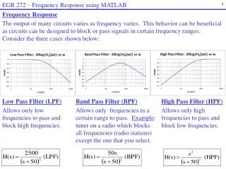
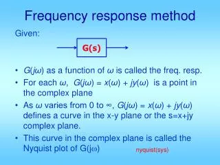
Frequency Response of Amplifier. Jack Ou Sonoma State University. RC Low Pass (Review). A pole: a root of the denomintor 1+sRC=0→S=-RC. Laplace Transform/Fourier Transform. (Laplace Transform). Complex s plane. | +p|. (Fourier Transform). -p. p=1/(RC).

E N D
Frequency Response of Amplifier Jack Ou Sonoma State University
RC Low Pass (Review) A pole: a root of the denomintor 1+sRC=0→S=-RC
Laplace Transform/Fourier Transform (Laplace Transform) Complex s plane |+p| (Fourier Transform) -p p=1/(RC) Location of the zero in the left complex plane )|=1/|+p| Phase=-tan-1(/p)
Rules of thumb: (applicable to a pole) Magnitude: 20 dB drop after the cut-off frequency 3dB drop at the cut-off frequency Phase: -45 deg at the cut-off frequency 0 degree at one decade prior to the cut-frequency 90 degrees one decade after the cut-off frequency
RC High Pass Filter (Review) A zero at DC. A pole from the denominator. 1+sRC=0→S=-RC
Laplace Transform/Fourier Transform (Laplace Transform) Complex s plane |+p| (Fourier Transform) -p p=1/(RC) Zero at DC. Location of the zero in the left complex plane )|=||/|+p| Phase=90-tan-1(/p)
Zero at the origin. Thus phase(f=0)=90 degrees. The high pass filter has a cut-off frequency of 100.
RC High Pass Filter (Review) R12=(R1R2)/(R1+R2) A pole and a zero in the left complex plane.
Laplace Transform/Fourier Transform (Low Frequency) (Laplace Transform) Complex s plane |+p| |+z| (Fourier Transform) -p z=1/(RC) p=1/(R12C) -z Location of the zero in the left complex plane At low frequencies, |+p|>|+p|.
Laplace Transform/Fourier Transform (High Frequency) (Laplace Transform) Complex s plane |+z| |+p| (Fourier Transform) -p z=1/(RC) p=1/(R12C) -z Location of the zero in the left complex plane At high frequency, |+p|is almost equal to |+p|.
Design • ωz=1/R1C • ωp=1/(R12)C • Note that R12<R1 • If R2<<R1, ωp/ ωp=R1/R2 • Design for ωp/ ωp=1000
Device Setup Gmoverid: Gm=17.24 mS RS=1000 Ohms GMBS=2.8 mS CGS=62.79 fF
Small Signal Parameters Design Constraints: 1/(gm+gmbs)=50 Ohms Large R1 to minimize Q R2=58 Ohms R1=1102 Ohms L=4.013 nH
Gm1=201.3uS GM3=201uS CGS3=CGS4=306.9fF GDS4=3.348uS GDS2=5.119uS Rload=118 Kohms Cload=1 pF Fp1=1.347 MHz Fp2=52.11 MHz Fz=104.2 MHz
Magnitude AvDC,matlab=27.52 AvDC,sim=27.45 Fp1matlab=1.34MHz Fp1sim=1.23 MHz
Understanding Transit Frequency Since fT depends on VGS-VT, fTdepndes on gm/ID. fT depends on L.
Overdrive Voltage as a function of gm/ID gm/ID=2/(VOV)
Trade-off of gm/gds and fT fT gm/gds gm/ID 15-20
Numerical Example VDS=0.6 V
Numerical Example VDS=0.6 V
Use to gm/ID principle to find capacitance • gm/ID→(fT,I/W,gm/gds) • fT=gm/cgg, cgg=cgs+cgb+cgd • cgs/cgg is also gm/ID dependent.
Example • Assume gm/ID=20, L=120 nm, VDS=0.6V, I=100uA. • fT=22.76 GHz • cgg=gm/fT=13.98 fF • cgd/cgg=0.29→cgd=4.1 fF • cgs/cgg=0.75 →Cgs=10.5 fF
Noise is not deterministic The value of noise cannot be predicted at any time even if the past values are known.
Average Power of a Random Signal Periodic voltage to a load resistance. Observe the noise for a long time. It is customary to eliminate RL from PAV. Unit: V2 rather than W.
Power Spectral Density Sx(f1) has unit of V2/Hz. PSD shows how much Power the signal carries at each frequency.
Correlated and Uncorrelated Sources Pav=Pav1+Pav2 Superposition holds for only for uncorrelated sources. (How similar two signals are.)
Uncorrelated/Correlated Sources (Multiple conversations in progress) (clapping)
Example Vnr1sqr=2.3288 x 10⁻¹⁹ Vnr3sqr=7.7625 x 10⁻²⁰ Vnoutsqr=3.1050 x10⁻¹⁹