Download
1 / 67
910 likes | 2.04k Views
Phase Locked Loop. 2008 년 11 월 7 일 전북대학교 전자정보공학부 정항근. Analogy to Spinning Tops. Reference. Tracking. Synchronized: same rpm & same facets. Analogy to motor speed control. Duty cycle of PWM signal. Switch setting. Control. Error. Set Point. Action. +. Motor. Controller. _.

E N D
Phase Locked Loop 2008년 11월 7일 전북대학교 전자정보공학부 정항근
Analogy to Spinning Tops Reference Tracking Synchronized: same rpm & same facets
Analogy to motor speed control Duty cycle of PWM signal Switch setting Control Error Set Point Action + Motor Controller _ PID controller Measured Speed
Rotating phasor Imaginary Real
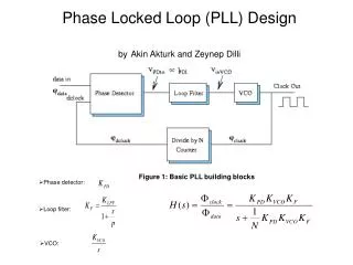
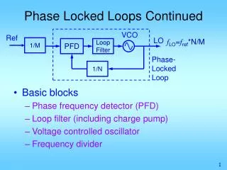
Basic Structure of a PLL • Phase Detector : generates a voltage proportional to the phase difference between the input and the output • Loop Filter : filters out undesirable frequency components • VCO (Voltage Controlled Oscillator): generates a periodic signal whose frequency is proportional to the control voltage
Basic operation of PLL • Negative feedback system: the phase of the input clock is compared to that of the VCO and the resulting phase error is filtered and drives the VCO to maintain an almost fixed phase error. • Phase lock means the frequencies of the input and VCO are the same, when the PLL is in lock.
What are PLLs for? Note that the PLL doesn’t just produce an exact duplicate of the input clock. We can accomplish some processing of the input clock signal. • Filtering : jitter reduction, clock recovery • Frequency scaling : frequency synthesis • Synchronization : skew reduction
Filtering • With LPF for the loop filter, high frequency fluctuation is blocked. • But the LPF allows the PLL to track the input frequency drift. • The PLL can be thought of as a tracking BPF.
Data regeneration in digital communication Amplifier & Equalizer Decision Circuit. Clock Recovery Clock recovery reduces the timing jitter in the retiming clock.
Frequency synthesis With a divider inserted between VCO and PD, we can generate harmonics of the input clock. Thus the PLL can be used to generate multiple channel frequencies based on a very stable reference oscillator.
Phase synchronization Clocks with proper phase alignment are critical to high speed data transfers. The PLL is useful for reducing skews. chip PLL clk clk Pclk Pclk clk clk Pclk Pclk
PLL as an FM demodulator PD LPF FM modulated signal with frequency fin VCO input voltage proportional to the frequency deviation from the VCO free running frequency ffr → FM demodulation VCO
Types of PLL • LPLL (Linear PLL): analog phase detector (multiplier), analog loop filter, analog VCO • DPLL (Digital PLL): digital phase detector, analog loop filter, analog VCO • All digital PLL: digital phase detector, digital loop filter, DCO
LPLL Analog Multiplier X Analog LPF VCO
DPLL Digital phase (frequency) detector Analog LPF VCO
Phase detectors • Generates a voltage whose average value is proportional to the phase difference between the two clocks • Averaging is done by the subsequent low pass filter block • Characterized by the conversion gain whose unit is in V/rad
y(t) x1(t) x2(t) Multiplier-type phase detector Quadrature nature of the multiplier-type PD can be taken into account for convenience. When the PLL is in lock,
Multiplier-type PD (cont’d) 1 . 0 0 . 8 0 . 6 0 . 4 0 . 2 - - 0 . 2 - 0 . 4 - 0 . 6 - 0 . 8 - 1 . 0
Exclusive OR-type PD The phase difference determines the duty cycle of the output pulse whose average is proportional to the phase difference. Note that the useful range is ±p/2 around ±p/2.
Exclusive-OR type PD (cont’d) • Exclusive-OR type of detectors exhibit the same quadrature phase relationship between the input and VCO as the multiplier type PDs. • Advantage of simple hardware • Two drawbacks • phase error limit of ± 90 degrees • Sensitive to the duty cycle, not just to the phase difference
Loop filter Suppresses the unwanted frequency components in the output of the PD before it reaches the VCO input Normally passes only slowly varying components and blocks the fast fluctuating components Also serves the averaging function needed for the PD
R C Loop filter (cont’d) Lag type It is the simplest filter, but has only one parameter for handling the conflicting requirements of the PLL.
Loop filter (cont’d) Lag-Lead type R1 R2 ,where t1=R1C, t2=R2C,z=1/t2 and p=1/(t1+t2). Thus we have one more parameter to vary to satisfy the specifications for the PLL. C
C R2 R1 - A + Loop filter (cont’d) Active PI type We now have DC gain. When the gain is infinite, the filter performs PI (Proportional-Integral) function.
Mathematical model for VCO Accounting for only the excess phase due to the control voltage change
Four frequency ranges Four ranges are defined for PLLs: • Hold range: the input frequency range in which a PLL can maintain the lock • Pull-in range: the input frequency range within which a PLL will eventually achieve the lock • Pull-out range: the maximum value of a frequency step in the input signal which causes the PLL to lose the lock • Lock range: the input frequency range within which a PLL achieves the lock within a single-beat note
Four frequency ranges (cont’d) ± DwL: lock range ± DwPO : pull-out range ± DwPI : pull-in range ± DwH : hold range
Kd F(s) Kv/s Loop modeling Linearized modeling in phase lock condition qe + qi qo - High frequency components of input jitter are reduced.
Transfer functions For the passive lag filter,
Transfer functions (cont’d) • Limitations of PLL with passive lag LPF: • Coupling between z, wn, and K=KdKv • If K is increased to reduce static phase error, then z decreases. • If wLPF (= 1/t) is decreased to reduce high-frequency jitter, then z decreases. • Finite DC loop gain causes large static phase error.
Transfer functions (cont’d) For the passive lag-lead filter, Note that one additional variable relaxes the tradeoff relationship.
Transfer functions (cont’d) For the active PI filter,
qe + qi qo - Kd F(s) Kv/s Phase error responses Phase error response Steady state phase error Inputs • - Phase step input • - Frequency step input • - Frequency ramp input
Transient response for phase step input Note that the linearized PLL model accounts for only the excess phase.
Transient phase error for phase step input For PI LPF,
Steady state phase error for phase step Since the frequency remains the same, there will be no change in the VCO control voltage, thus no change in the phase error after the transient settles down.
Transient response for frequency step input Note that the linearized PLL model accounts for only the excess phase.
Transient phase error for frequency step input For PI LPF,
qi + F(s) Kd qe - Kv qo wo --> wo +Dw Steady state phase error for frequency step
R C R2 C R1 - A + Steady state phase error: passive vs. active filters Passive filter Active filter A ~ large
qo qi G(s) - |G(jw)| dB wT wp log w G.M. -90o P.M. -180o System stability Negative feedback system In PLLs, G(s)=KdKvF(s)/s Gain margin and phase margin
+ qo qi - Kd Kv/s |G(jw)| Slope= -20dB/dec wT=K=KdKv -90o Bode plot: 1st order PLL Phase margin : 90o ==> stable
Kd Kv/s Bode plot: 2nd order PLL with PI-type LPF qe + qo qi (1+st2)/st1 - |G(jw)| |G(jw)| -40dB/dec -40dB/dec -20dB/dec 1/t2 1/t2 -20dB/dec -90o -90o -135o P.M. -135o -180o P.M. -180o Enough P.M. : stable Low P. M. : unstable