Download
1 / 72
930 likes | 1.61k Views
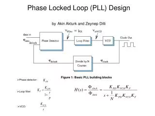
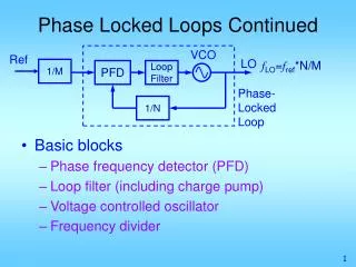
Phase-Locked Loop. Phase-Locked Loop in RF Receiver. Antenna. BPF1. LNA. BPF2. Mixer. BPF3. IF Amp. Demodulator. RF front end. LO. VCO. Ref. PD. Loop Filter. Phase-Locked Loop. 1/N. Functional Blocks in PLL. Phase detector (PD): find difference between phases of two signals

E N D
Phase-Locked Loop in RF Receiver Antenna BPF1 LNA BPF2 Mixer BPF3 IF Amp Demodulator RF front end LO VCO Ref. PD Loop Filter Phase-Locked Loop 1/N
Functional Blocks in PLL • Phase detector (PD): find difference between phases of two signals • Loop filter: provide appropriate control voltage for the voltage-controlled oscillator (VCO) • VCO: generate signals with phase determined by the control voltage • Divide-by-N: LO phase changes N times faster than Ref phase VCO Ref LO PD Loop Filter Phase-Locked Loop 1/N
Design Issues • Tracking behavior • Noise performance • Jitter characteristics • Jitter tolerance • Jitter transfer • Jitter generation • Power consumption
System Modeling • vRef: input reference signal • vLO: local oscillator (LO) output signal • vd: detector output • F(s): transfer function of loop filter • vC: control voltage for VCO VCO vd vC vRef PD F(s) vLO
System Modeling • Phase signals contain information • qRef: phase of reference signal • qLO: phase of local oscillator (LO) signal • qe: phase difference between qRef and qLO qRef VCO Kdqe vRef PD F(s) vLO qLO
Phase Detector • Vd=Kdqe=Kd(qREF – qLO) • Kd: gain of phase detector qREF+ qe vd Kd - qLO
Loop Filter • VC(s) = F(s) Vd(s) • Low-pass filter • Extract phase error • Remove high frequency noises • Passive filter for integrated PLL • Active filter for discrete component PLL vd vC F(s)
Passive Lag Filter R1 + + R2 vd vC C – – • Lag filter: pole magnitude smaller than zero • Passive components: high linearity, gain < 1
Active Lag Filter R1 C1 R2 C2 + + – vd vC + – – • Can adjust pole and zero locations • Can have gain • Op amp limitations
Active Proportional-Integral (PI) Filter R1 R2 C + + – vd vC + – – • Large open loop gain at low frequency • Op amp limitations • Linearity • Noise • Open loop gain
Voltage-Controlled Oscillator • KVCO: gain of VCO vC qLO + KVCO 1/s + w0
Transfer Function of PLL • Open-loop transfer function from qe to qLO w0 + qREF+ qe vd vC qLO + Kd F(s) KVCO 1/s - qLO
Transfer Function of PLL • Closed-loop transfer function from qREF to qLO w0 + qREF+ qe vd vC qLO + Kd F(s) KVCO 1/s - qLO
Transfer Function from qREF to qe • Closed-loop transfer function w0 + qREF+ qe vd vC qLO + Kd F(s) KVCO 1/s - qLO
Other TF of Interest • Noise in control voltage vCn + qREF+ qe vd vC qLO + Kd F(s) KVCO 1/s - qLO
Other TF of Interest • Phase noise of VCO qn + qREF+ qe vd vC qLO + Kd F(s) KVCO 1/s - qLO
Transfer Functions for Different Loop Filters • Passive lag filter • Active lag filter • Active PI filter
Normalizing Transfer Function • Normalized denominator • Passive lag filter • Active lag filter • Active PI Filter
Normalized Transfer Function • Passive lag filter • Active lag filter • Active PI Filter
Normalized Transfer Function • Passive lag filter • Active lag filter
Step Response of PLL • Phase step • Phase Error • Steady state error (final value theorem)
Ramp Response of PLL • Phase ramp • Phase Error • Steady state error (final value theorem)
General Steady State Error in Ramp Response • High loop gain • Low loop gain
Stability of PLL • Criterion for stability • Closed-loop pole at left half plane • Sufficient phase margin • Control of pole location • Open loop gain • Open loop zero • Check root locus
Root Locus Method • Closed-loop TF • Closed-loop poles make • K=0, open-loop poles • K infinity, open-loop zeros or infinity
Phase Noise and Jitter • Phase noise • Fluctuation in phase • Frequency domain • Discussed in RF circuits • Jitter • Error in clock edge (period) • Time domain • Significant in communications circuits • Two concepts • Related to each other • Exact relationship not clear
Jitter Measurements Agilent, “Understanding Jitter and Wander Measurements and Standards.”
Jitter Tolerance • Ability of a PLL to operate with jitter • Applied to its reference • Various magnitudes • Different frequencies • Usually specified using an input jitter mask • Jitter magnitude and corner frequencies • BER requirement • Various for standards
PLL in Clock and Data Recovery 0 1 0 0 1 0 1 0 1 Ideal signal Distorted signal 0 1 0 0 X 1 0 1 0 Ideal clock 0 1 0 0 1 0 1 0 Recovered clock
Jitter Tolerance Measurement • Error at corner frequency • Insufficient clock recovery bandwidth • Incorrect mask used
Jitter Tolerance Measurement Tolerance margin • Excessive jitter tolerance margin
Jitter Tolerance Measurement • Occasional fail at specific frequencies • Need extra settling time after jitter amplitude change • Repeating with additional settling time • Spot measurement
Jitter Tolerance Measurement • Limited clock recovery bandwidth • Eye-width alignment noise