Download
1 / 11
120 likes | 306 Views
Technical University of Sofia. An Educational Electronic Prototype System for Phase-Locked Loop Based Circuits Eltimir Stoimenov (1) , Iv а ilo Pandiev (2) e_stoimenov@tu-sofia.bg (1) , ipandiev@tu-sofia.bg (2). Our objective:

E N D
Technical University of Sofia An Educational Electronic Prototype System for Phase-Locked Loop Based Circuits EltimirStoimenov(1), IvаiloPandiev(2)e_stoimenov@tu-sofia.bg(1), ipandiev@tu-sofia.bg(2)
Our objective: To develop a laboratory stand which helps students to understand the basics of the PLL circuits.Why? Because PLL circuits are widely applied in communication, electronics and computer sciences. In this order students should possess a high level of knowledge in the PLL theory.
What we have done: • We have designed a versatile educational PLL stand which incorporates the most important applications of the PLL circuits: • phase locking; • frequency synthesis with integer and • non-integer coefficients; • frequency demodulation.
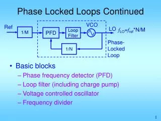
FM generator LPF_1 LPF_2 PWM_OUT DEM_OUT R3 R4 C2 P C3OUT P C1OUT P C2OUT P CPOUT VCOIN FREQUENCY DIVIDER 1 0 - 512 INPUT IN SIGIN PC VCO OUT PLL 4046 OUTPUT VCOOUT COMPIN R1 R2 C1A C1B • FM generator: • Allows frequency demodulation • - Central frequency: 0-1MHz; • Adjustable deviation; • Adjustable data signal frequency. • Data signal PWM output • Based on MSP430F5310 R1 R2 C1 • Frequency dividers: • Allows frequency synthesis • Programmable coefficients • 9bits resolution • Based on MSP430G2553 • Low Pass Filter: • Lag-lead type (one pole, one zero); • Allows the students to set the capture range • PLL circuit: • Based on 4046 IC • Students can set the VCO parameters by external components FREQUENCY DIVIDER 2 0 - 512 OUT IN
Experimental results LPF_3 FM generator LPF_2 PWM_OUT DEM_OUT LPF_1 P COUT VCOIN FREQUENCY DIVIDER 1 0 - 512 INPUT IN OUT SIGIN PLL 4046 OUTPUT VCOOUT COMPIN FREQUENCY DIVIDER 2 0 - 512 OUT IN - PWM output 2. Frequency demodulation 1. Frequency synthesis
Laboratory stand part -1 Laboratory stand part -2
Exercise set, part 1: • 1. Study the Phase-Loop-Locked circuit realized with 4046 IC. Consider the following input parameters: • - VCO central frequency – fO = 100 kHz for VVCOIN= 1/2VCC; • - Lock range - 2fL = 100 kHz; • - Settling time – tset = 1 ms for maximum ripples ≤ 5% ; • - Overshoot ≤ 20% and settle to within 5% at wnt = 5. • 2.Calculate all the external VCO components – R1, R2 and C1. Calculate the values of the LPF_1 components - R3, R4 and C2. For the calculation use the nomograms and formulas given 4046 datasheet from Philips. • 3. Set the components values according the calculation you made in the previous point. Apply a square wave signal of 5 V magnitude and frequency of 100 kHz. The frequency dividers and the FM generator should not be connected to the circuit. • - Measure the VCO controle voltage – VCOIN; • - Use an oscilloscope to observe the input and the output signals. Measure the frequencies of the signals; • - Determine the width of the lock range. Find the fMIN and fMAX frequencies and measure the corresponding VCO control voltages. Compare the values with the input parameters.
Exercise set, part 2: 4. Synthesize output signals with frequencies of 90 kHz to 110 kHz with step of 1 kHz. In this order connect the two frequency dividers to the PLL circuit and change the division coefficients appropriately. Apply a square wave input signal of 5V magnitude and frequency of 1 kHz. The FM generator should not be connected to the circuit. 5. Realize a frequency demodulator using the PLL circuit. For this purpose connect the FM generator to the input and by using the rotary encoder adjust the signal as follows: carrier signal central frequency: 100 kHz; deviation: ±40%; data signal frequency: 100 Hz. Connect the VCOIN signal to LPF_2 input and observe the demodulated signal in the LPF_2 point. The original data signal is also PWM modulated and after filtering it can be observed in PWM_OUT point. Compare the two signals. The frequency dividers should not be connected to the circuit.
THE PILOT TEST The pilot test of the developed educational prototype system will be performed in 2012 with hundred of 3rd year regular students within 24 learning hours. In particular the educational system is a part of the laboratory practice of the Mixed-signal system course. The evaluation of the system will be focused on usability of the learning material, instructional effectiveness and learners’ attitudes. The chosen block structure provides possibilities for future extension of the developed system with additional elements and functionality.
CONCLUSIONS The developers’ team achieved the following results of the of the : - Development of a procedure for PLL circuits study; - Development of an educational electronic prototype system based on monolithic PLL 4046. The created system allows to study some of the basic PLL circuit applications, such as phase locking process, frequency synthesis and frequency demodulation; - Creating students’ guide and assignments for supporting the created educational prototype system.
Thank you for your attention For more information please contact us on: e_stoimenov@tu-sofia.bg