Download
1 / 151
1.6k likes | 2.13k Views
E771 Electronic Circuits III Phase-locked loop notes. by Paul Brennan. University College London. Prepared 2000. Contents. 1 Introduction 2 Loop Components 3 The Second Order Type II Loop 4 Modulation Characteristics 5 Noise Performance 6 Acquisition 7 Higher Order Loop Filters

E N D
E771 Electronic Circuits IIIPhase-locked loop notes by Paul Brennan University College London Prepared 2000
Contents 1 Introduction 2 Loop Components 3 The Second Order Type II Loop 4 Modulation Characteristics 5 Noise Performance 6 Acquisition 7 Higher Order Loop Filters 8 Other Applications Examples and solutions Please note that material which is provided for reference only and is not an essential part of the course is distinguished by a vertical line in the left-hand margin.
Best, R.E., “Phase-locked loops, theory, design and applications”, McGraw Hill, 1993. Brennan, P.V., “ Phase-locked loops: Principles & Practice”, Macmillan, 1996. Gardner, F.M., “ Phaselock techniques”, 2nd ed., Wiley, 1979. Rohde, U.L., “ Digital PLL frequency synthesisers”, Prentice Hall, 1983. Some useful books
Phase-locked loops (PLLs) are widely used in a variety of applications. These include line synchronisation and colour sub-carrier recovery in TV receivers, synthesised local oscillators and FM demodulators in radio receivers and frequency synthesisers in transceivers and signal generators, to name but a few. Although the basic operation of PLLs appears quite straightforward, the detailed design of a PLL for a particular application often requires a great deal of understanding of their underlying principles of operation and associated limitations. It is very easy to design a PLL badly by ignoring basic control loop considerations or by attempting to make short-cuts. For these reasons, and because PLLs usually employ a collection of RF circuit design techniques, these notes consider - in some detail - the principles and capabilities of PLLs and their basic design procedures. 1. Introduction
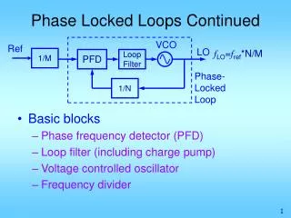
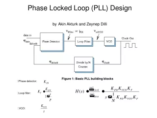
1. Introduction A PLL is a control loop consisting of four fundamental components, as shown in figure 1. These are a phase detector (sometimes called phase comparator), loop filter, voltage controlled oscillator (VCO) and a frequency divider. These components are connected in a simple feedback arrangement so that the phase detector compares the phase, fi, of an input signal with the phase, fo/N, of the fed-back output signal. The phase detector output voltage is dependent on the difference in phase of the two applied inputs and is used to adjust the VCO until this phase difference is zero. The loop is then in a stable equilibrium so that the VCO phase is locked to the input signal phase, fo = Nfi. Thus the circuit behaves as a phase multiplier and also, since frequency is the time derivative of phase, as a frequency multiplier.
The behaviour of a PLL can be likened to that of a feedback voltage amplifier such as that shown in figure 2. This is the block diagram representation of a non-inverting op-amp voltage amplifier, where the output and input voltage are related by Vo = KVi. It is similar to the basic PLL except that it uses a voltage comparator instead of a phase comparator, a potential divider in the feedback instead of a frequency divider and the controlled parameter is voltage rather than phase. The analogy between these two circuits has been drawn to illustrate that PLLs are simply a type of control loop in which the parameter under control happens to be the phase of a number of signals. 1. Introduction
1. Introduction The active characteristics of PLLs are governed by the loop filter design. A narrow loop bandwidth is needed in applications where the input signal is noisy - such as with FM discriminators or carrier-recovery circuits. A principal attraction of PLLs is that the loop bandwidth may be made very narrow so that the loop can recover signals buried in noise and yet still track their frequency variations over a wide range. On the other hand, a wider bandwidth is needed in applications requiring higher operating speed, such as agile frequency synthesisers and there are also certain practical constraints on the loop characteristics. These points are illustrated in these notes.
2. Loop components The four main loop components of figure 1 shall now be described in more detail. • Phase detectors Phase detectors are a form of comparator providing a DC output signal proportional to the difference in phase between two input signals. This may be written, where Vp is the output voltage, fi1 and fi2 are the phases of the input signals and Kp is the phase detector gain in Volts per radian. In general, the response of phase detectors is non-linear and repeats over a limited phase range. However the response is usually very nearly linear in a narrow phase range close to the point at which the loop would lock and the value of phase detector gain is only of real interest at this point. (1)
There are two basic types of phase detector, multiplier and sequential. Multiplier types form the analogue product of two input signals, the DC component of which is dependent on the phase difference between the inputs. Sequential types respond to the relative timing of the edges of the input signals and are usually implemented in digital form. The multiplier type, being linear, are useful in applications where the input signal is noisy, since the output S/N ratio degrades at the same rate as the input S/N ratio. The sequential type are vulnerable to poor operation under low S/N conditions and would normally be used at S/N ratios significantly above 10 dB. However, they can offer far superior capture and tracking performance. 2. Loop components The simplest example of a multiplier type phase detector, which is actually very widely used, is the analogue multiplier of figure 3. This is basically a double-balanced mixer (or four quadrant multiplier) with a DC coupled output port, that is used to produce the product of two input signals V1(t) and V2(t). Of course, a standard double-balanced mixer (with a DC coupled IF port) could be used as such a phase detector although mixers are produced especially for this purpose with low DC offsets and high sensitivity - both of which are important characteristics of multiplier type phase detectors.
2. Loop components Operation can be easily understood by considering sinusoidal input signals, V1(t) = V1coswt and V2(t) = V2cos(wt - f), the phase detector output being proportional to the product of these signals,
2. Loop components Thus the output consists of a DC term and a double-frequency component. The double-frequency component is filtered out by the action of the loop filter and is of no significance, leaving (2) This shows that the phase detector output varies sinusoidally with phase difference, with zeros at f = p/2 + np. The loop therefore locks, with this particular type of phase detector, when there is a quadrature phase difference between the phase detector inputs.
2. Loop components Phase detector gain is given by and in the linear regions of the characteristic, around f = p/2 + np, the gain in V/rad is So the phase detector gain is equal to the peak value of output voltage. The useable range of the detector is limited to within ±p/2 rads of f = p/2 + np. Analogue multiplier type phase detectors are often used with one square-wave input signal and one sinusoidal input signal. This is often for reasons of convenience since the frequency divider and maybe also VCO are implemented in digital circuitry. In this case, for relatively low frequency operation (up to around 1 MHz), the circuit of figure 4 is useful.
2. Loop components This performs exactly the same function as an analogue multiplier driven by one analogue signal and one digital signal, but has the advantage that it requires no multiplying components. The circuit works simply by acting as a unity gain inverting amplifier when the digital input is high and a unity gain non-inverting amplifier when the digital input is low. The performance of this mode of operation of analogue multiplier phase detectors is best explained with reference to the timing diagrams of figure 5. Here the inputs are shown as a sinewave of amplitude V1 and a square-wave, lagging by f, of amplitude V2.
2. Loop components When the square-wave input is high the sinusoid is non-inverted and when it is low the sinusoid is inverted. Thus the phase detector output is a double-frequency sample of a sinusoid, cosq, over the range q = f - p/2 to q = f + p/2. This signal has an obvious DC component which is dependent on the phase difference, f, as follows (3) from which it is clear that the response is sinusoidal, as before, with a phase detector gain of Kp = 2KV1V2/p V/rad. At this point it should be noted that successive half-cycles of the output waveform of figure 5 are identical only if a square-wave of 50% duty cycle is used - and this is the optimum duty cycle for this type of phase detector. The phase detector may also be used with square-wave signals applied to both inputs, as shown in figure 6. The output signal is now a series of positive pulses of width Dq = p - f and negative pulses of width Dq = f (for 0 ≤ f ≤ p as shown in the diagram).
2. Loop components Thus the phase detector characteristic is given by (5) The response is now a triangular waveform with the advantage that it is linear over the full ±p/2 rads operating range of the detector. This allows an improvement in the capture and holding performance of the loop. From equation (5), the phase detector gain is now Kp = 2KV1V2/p V/rad. From figure 6 it can be seen that an analogue multiplier with square-wave inputs performs an exclusive-NOR logic function. Thus, in circuits containing mostly logic components, it may be preferable to use a single exclusive-OR (or exclusive-NOR) gate as such a phase detector, as shown in figure 7. It should be noted that, since the output voltage of an exclusive-OR phase detector varies between the two logic levels and does not have a zero mean value, a DC offset equal to the mean of the logic "1" and logic "0" levels needs to be provided at the loop filter for the detector to function correctly.
2. Loop components The characteristics of analogue multiplier phase detectors used in their various modes of operation are summarised in figure 8. In a PLL, lock occurs when the phase detector output is zero and when the polarity of the feedback path through all the loop components is negative. Since the loop filter is usually based on an op-amp integrator with a phase inversion at DC this means that the basic loop of figure 1 locks on a positive slope of the phase detector characteristic, i.e. when fo/N - fi = -p/2. Multiplier phase detectors have the useful property that when one input signal disappears the mean output is zero. In PLLs using integrating filters (which is the majority of practical loops) this enables the loop to "flywheel" during a temporary loss of signal and rapidly regain lock when it returns - a technique used in colour TV sets.
2. Loop components Analogue multiplier phase detectors with square-waves applied to one or both inputs are capable of responding to odd harmonics in addition to the fundamental frequency. This enables the loop to be locked to an odd harmonic (or sub-harmonic) of the input signal, if desired. The behaviour of an exclusive-OR type of phase detector presented with inputs of frequency w and 3w is illustrated in figure 9.
2. Loop components The output signal can best be thought of as a successively inverted and non-inverted version of the 3rd harmonic input signal, the inversion being controlled by the fundamental input signal. It is clear that the detector output signal has a mean DC level that varies with the phase difference between the two applied inputs. The relative phase of the two input signals shown in figure 9 has been deliberately chosen to produce maximum DC response from the detector and it can be seen that this is one third of the maximum response that would be obtained from input signals of equal frequency. Thus, the phase detector gain is reduced by a factor of three. By considering a series of diagrams such as figure 9 it is apparent that, for input signals of frequency w and nw, the phase detector characteristic is triangular, as before, but the output signal level - and hence phase detector gain - is reduced by a factor of n. In practice, a further reduction in gain occurs due to the finite rise time of the square-wave edges. Any practical phase detector has a small DC offset in its output voltage due to component tolerances and this may have an adverse effect on PLL performance, perhaps even preventing the loop from locking. The effect is much more serious in harmonically operated phase detectors since the output level is reduced by at least a factor of n and so any DC offset is much more significant. It can therefore be quite tricky to achieve high order harmonic locking in PLLs and very careful minimisation of the phase detector DC offset is required.
2. Loop components (a) (b) Figure 9a(bonus figure) Phase detector output waveforms with (a) 3rd harmonic and (b) 5th harmonic locking.
2. Loop components The phase detectors described so far produce an AC output signal in addition to the desired DC component. This alternating signal has a fundamental frequency of twice the applied signal frequency. When such phase detectors are included in PLLs, the alternating component of their outputs can tend to modulate the VCO frequency producing unwanted sidebands on the output signal, often called reference sidebands. To minimise this effect, the loop natural frequency is constrained to well below the frequency at which the phase detector operates (usually around 100 times lower). However, there is a different type of multiplying phase detector known as a sample-and-hold detector which, in principle, produces no alternating components in its output. As its name implies, it is based on a sample and hold circuit in which one phase detector input is a digital signal, the rising edges of which are used to determine the sampling instants of the other sinusoidal input. This produces a sinusoidal phase detector characteristic. The resulting output signal contains just a small amount of second harmonic ripple due to "drooping" in the holding capacitor. Sample-and-hold detectors enable significantly higher loop natural frequencies to be used without producing severe reference sidebands.
2. Loop components Figure 9b (bonus figure) Sample and hold phase detector.
2. Loop components We shall now look at two common types of sequential phase detector...
2. Loop components Probably the simplest example is the RS flip-flop phase detector which is illustrated in figure 10. Its operation is very easy to understand by considering two digital input signals of phase difference f. The flip-flop is set on the rising edge of input 1 and is reset on the rising edge of input 2. The duty cycle of the flip-flop output and the associated mean DC level is thus an indication of the phase difference between the two input signals. The mean DC level varies linearly between the logic "0" output voltage level, VOL, when f = 0 to the logic "1" output voltage level, VOH, when f = 2p rads and this characteristic is plotted in figure 11. In practice, a DC offset of (VOL + VOH)/2 would need to be introduced at the loop filter and a PLL incorporating this phase detector would lock at a phase difference, f, of p rads. This phase detector has a linear range of 2p rads - twice that of an exclusive-OR phase detector and so has an improved capture and holding characteristic. Being a sequential phase detector it responds only to the rising edges of the input signals, so their duty cycle is immaterial, although it is far less tolerant of input noise than multiplier phase detectors. Also, in the absence of an input signal the mean output latches-up in one state, thus preventing the detector being used in a flywheel type of PLL.
2. Loop components A more widely used type of sequential phase detector is the phase/frequency detector of figure 12. This is available in integrated circuit form although it may be constructed from a pair of D-type flip flops and an AND gate as shown in the diagram.
2. Loop components Its operation is a little more subtle than the RS flip-flop phase detector. Referring to figure 13, assuming initially that input 1 leads input 2 by an amount f, then after each rising edge of input 1 the Q1 output is set to logic "1". When the next rising edge of input 2 is received, for an instant both Q1 and Q2 outputs are set to logic "1". This produces a pulse on the reset inputs of the flip-flops which are then both reset to logic "0". Thus, if input 1 leads input 2 then the mean value of the Q1 output indicates the amount of phase lead in the same way as the RS flip flop detector, whilst the mean value of the Q2 output is virtually VOL. Conversely, if input 1 lags input 2 then the Q2 output becomes active and indicates the amount of phase lag. By summing these two outputs in a differential amplifier, a phase detector characteristic with a linear range of 4p rads is obtained, as plotted in figure 14. A practical advantage of this arrangement is that compensation for offsets in the logic levels is implicit in the use of a differential amplifier. If R2 = R1 then the phase detector output voltage varies between -(VOH - VOL) and + (VOH - VOL) passing through 0 when f = 0 as shown in figure 14. This is a particularly useful characteristic allowing the VCO and input signals to be in-phase in a locked PLL.
2. Loop components It should be noted that the differential amplifier is not expected to respond to the pulses in the detector output, but merely to the DC component. Usually, a differential form of loop filter would be used to achieve the functions of both a filter and differential amplifier. The AC component of the phase detector output is a series of short pulses at the operating frequency, giving rise to reference sidebands (in a badly designed loop) at the reference frequency and its harmonics. The most interesting feature of the phase/frequency detector is its behaviour with input signals of different frequency where, in contrast to multiplier phase detectors, it is able to discriminate between differing input frequencies.
2. Loop components Figure 14a (bonus figure) Operation of the phase/frequency detector with non-equal input frequencies.
2. Loop components If input 1 and input 2 are of frequencies w1 and w2, respectively, and w1 > w2, then the Q1 output is active whilst the Q2 output is a succession of short pulses with a mean value of virtually VOL. The probability that a rising edge of input 2 occurs between successive rising edges of input 1 is simply w2/w1 and its position between successive edges varies uniformly, on average being in the centre. Thus there is a (1 - w2/w1 ) probability that the Q1 output will not be reset between successive rising edges - giving maximum mean value during that cycle - and an w2/w1 probability that the Q1 output will be reset - giving, on average, 50% of the maximum value. The response is therefore Using similar arguments, for w1 < w2 the result is (6) (7)
2. Loop components The characteristic, shown in figure 15, is interesting in that there is a discontinuity at w1/w2 = 1 indicating that, if the input frequencies differ just slightly the detector produces half its maximum output voltage. This is due to the changeover between active outputs around the point where the input signals are nearly in-phase. This clear frequency discrimination characteristic makes the phase/frequency detector very useful in PLL applications where the loop is required to pull into lock from a large initial frequency offset and for this reason it is probably the most commonly used type of phase detector.
2. Loop components Figure 15a (bonus figure) Comparison of multiplier & sequential phase detectors
2. Loop components • Frequency dividers One of the most common uses of PLLs is in frequency synthesisers, where a range of output frequencies are generated from a single stable frequency reference. This requires the use of a variable ratio divider in the feedback path. There are other applications where fixed dividers are sufficient, such as in phase modulators or demodulators where a deviation beyond the range of the phase detector is needed, or in microwave frequency multiplier loops. It should be noted that frequency dividers act equally as phase dividers, so that a factor of 1/N must be allowed for in the loop equations. The basic arrangement of a high frequency programmable divider is shown in figure 16. It uses a high frequency fixed-ratio prescaler dividing the input frequency by a factor of P, followed by a programmable counter dividing the frequency by a further factor of N, the total division ratio being NP. The duty cycle of the output signal of fixed-ratio prescalers dividing by an even number is normally 50%, whereas the duty cycle of the output signal of other prescalers and of programmable counters may be far from 50%. This fact limits the use of many programmable counters to PLLs with sequential phase detectors, which is fine in the majority of applications.
2. Loop components ~5 GHz ~100 MHz The disadvantage of a PLL using this basic divider arrangement is that its output frequency is stepped in increments of P times the input or reference frequency. So, for a given output frequency increment, the reference frequency must be P times lower and this places more severe constraints on the loop natural frequency and hence loop performance. In particular, it increases the tuning time - which may be important in agile synthesiser applications - and it reduces the amount by which the VCO phase noise may be suppressed by locking to a clean reference signal. An improved divider scheme, known as dual-modulus prescaling, is shown next...
2. Loop components This makes use of a high frequency divider which divides by (P + 1) when the modulus control input is low and P when the modulus control input is high. A special low frequency counter is used to control the division ratio of the prescaler and consists of two programmable counters and some control logic. The two counters are initially loaded with the values N and A, where N ≥ A, and the modulus control signal is low so the prescaler divides by (P + 1). The counters are both decremented after each rising edge of the prescaler output until the A counter reaches zero. The modulus control signal then becomes high and the prescaler divides by P until the contents of the N counter reach zero, at which time the counters are reset and the cycle begins again. The division ratio is therefore Thus, by varying A from 0 to (P - 1), any integer value of division ratio is obtainable using this technique (subject to Nt(min) = P(P - 1)). This is a major advantage over the divider of figure 16 and, in frequency synthesiser applications, enables the output frequency to be stepped in increments of the reference frequency. Common prescaler ratios are 8/9 - allowing 3 A bits to be grouped with the N bits and treated as a single binary input and 10/11 - allowing a binary-coded-decimal representation of the division ratio. The more detailed timing considerations can be understood with reference to the example of figure 18 where N = 5, A = 3 and P = 4. (8) Nt = A(P + 1) + (N - A)P = NP + A, where N ≥ A.
2. Loop components The N and A counters are initially loaded with the values of 5 and 3, respectively, and are decremented after each rising edge of the prescaler output. When A = 3, 2 and 1 the prescaler divides by 5 and when N = 2 and 1 it divides by 4, giving a total division ratio of 23. The output signal is derived from the short pulse used to reset the counters. It is important to note that the prescaler division ratio is determined by the state of the modulus control on the rising input edge when the prescaler output is about to become high. Thus the modulus control signal should be triggered by the prescaler output edge prior to the counter state in which the division ratio needs to be changed, i.e. A = 1 and N = 1. This arrangement allows the relatively low frequency counter and modulus control logic the maximum possible time in which to change the state of the modulus control - P or (P + 1) periods of the input signal. In practice, look-ahead decoding is often used to further increase the speed of operation. The division ratio of dual-modulus prescalers can be increased using an arrangement such as that of figure 19. Dual modulus prescalers are usually designed with this in mind and include several modulus control inputs so that the external OR gate shown in the figure is not actually required.
2. Loop components The prescaler is followed by a ÷4 switch-tail divider, the two outputs of which are used as modulus control inputs. In three of the four possible flip-flop states the modulus control is thus held high and the prescaler is forced to divide by P. However, in the state before the Q2 output becomes high, the modulus control level is determined by the external control input and thus the prescaler division ratio of the next cycle may be P or (P + 1). The circuit therefore functions as a ÷4P/4P + 1 prescaler. It is important, from the timing considerations mentioned previously, that the modulus control input is active at the time when the Q2 output is about to become high. This point is often overlooked in data books and erroneous circuits are shown. A further type of frequency divider which has applications in agile synthesisers, is known as a fractional-N divider. This, as the name implies, is capable of dividing by a fractional number. In reality however, it actually toggles between two successive integers to provide a mean division ratio somewhere in between. This type of divider produces a large amount of sawtooth modulation at the reference frequency which is reduced by applying a similar waveform to the loop filter input (or by using sigma-delta techniques).
2. Loop components • Voltage-controlled oscillators (VCOs) VCOs are electronically tunable oscillators in which the output frequency is dependent on the value of an applied tuning voltage. They are realised in many forms from RC multivibrators at low frequencies to varactor and YIG-tuned oscillators at higher frequencies. As far as the loop filter design is concerned, the most important property of VCOs is their tuning characteristic. The slope of this characteristic, the VCO gain, is a further factor to be included in the loop equations, in addition to the phase detector gain, Kp, and divider ratio, 1/N, and is defined as (9) where wo is the output frequency and Vt is the tuning voltage. A typical tuning characteristic is shown in figure 20, where it should be appreciated that units of rad/s/V would normally be used in loop calculations for compatibility with the units of the phase detector gain.
2. Loop components It can be seen that, as the tuning voltage is increased, the VCO frequency initially increases rapidly and then increases more gradually. The VCO gain therefore decreases as the operating frequency is increased. Typically, the VCO gain may be expected to vary by a factor of two in a varactor-tuned oscillator having a tuning range of around half an octave. This is compounded in frequency synthesiser applications by the 1/N variation in frequency divider gain. In practice, some means of compensation would usually be provided for significant variations in loop parameters with operating frequency. This may take the form of a non-linear DC amplifier placed before the VCO, or a loop filter with gain related to the division ratio. A further important property of VCOs in PLL applications is their degree of phase noise purity (although amplitude noise is not important since this may be removed by limiting). This is a complex subject, although it is fair to say that spectral purity is dependent largely on the Q of the resonant element in the oscillator. In a loop having a wide bandwidth, a significant improvement in the residual VCO phase noise may be obtained by locking to a stable reference frequency - derived, perhaps, from a quartz crystal oscillator.
2. Loop components • Loop filters Operation of the PLL of figure 1 may be represented by the signal flow graph shown in figure 21. Here the filter transfer function is represented, using Laplace notation, by G(s) and a 1/s term is included to translate the VCO output frequency, wo, into phase, fo. The closed-loop transfer function may be found from Mason’s rule which reduces to the following for a single-loop control system,
2. Loop components The closed-loop transfer function is therefore, (10) Loops are categorised according to their order and type, the definitions being borrowed from control theory. The order of a loop is defined by the highest power of s in the denominator of the closed-loop transfer function shown above and the type of loop is defined by the number of perfect integrators within the loop. All loops are at least type I because of the integrating action of the VCO. The simplest loop is obtained when G(s) = 1 for which the transfer function is (11)
2. Loop components This is clearly a first order type I loop and the loop transfer function is simply a first order low-pass response with a time constant of N/(KpKv). This loop is of very limited practical use since there is no filtering of the phase detector output. An improvement can be obtained by using a passive low-pass filter, but this also has limitations such as there being a finite phase offset necessary to support a steady-state VCO control voltage and possible acquisition and tracking problems. More useful loop filters fulfil a combination of low-pass and integrator properties, the latter function requiring the use of an active device such as an op-amp. In practice, virtually all designs include active loop filters since little, if anything, is to be gained from their passive counterparts. Figure 21a (bonus figure) First order low-pass filter, showing identical response to a first order type 1 PLL..
3. The second order type II loop One of the most useful and popular designs of loop filter, producing a second order type II response, is shown in figure 22. It functions as an integrator at low frequencies with a DC gain equal to that of the op-amp. Since this gain is very high it may be regarded as a perfect integrator at DC, for which the filter transfer function is (12)