Download
1 / 19
220 likes | 713 Views
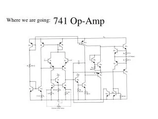
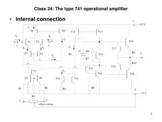
The 741 opAmp. DC and Small Signal Analysis. Jeremy Andrus For Engineering 332 May 15, 2002 Prof. Ribeiro. Overview: Five Parts of the 741. Biasing Currents Input Stage Second Stage Output Stage Short Circuit Protection. Overview: 741 Schematic. Biasing Current Sources.

E N D
The 741 opAmp DC and Small Signal Analysis Jeremy Andrus For Engineering 332 May 15, 2002 Prof. Ribeiro
Overview: Five Parts of the 741 • Biasing Currents • Input Stage • Second Stage • Output Stage • Short Circuit Protection
Biasing Current Sources • Generates the reference bias current through R5
Biasing Current Sources:DC Analysis • The opAmp reference current is given by: • For Vcc=Vee=15V and VBE11=VBE12=0.7V, we have IREF=0.73mA
Input Stage • The differential pair, Q1 and Q2 provide the main input • Transistors Q5-Q7 provide an active load for the input
Input Stage:DC Analysis - 1 • Assuming that Q10 and Q11 are matched, we can write the equation from the Widlar current source: • Using trial and error, we can solve for IC10, and we get: IC10=19A
Input Stage:DC Analysis -2 • From symmetry we see that IC1=IC2=I, and if the npn is large, then IE3=IE4=I • Analysis continues:
Input Stage:DC Analysis -3 • Analysis of the active load:
Second (Intermediate) Stage • Transistor Q16 acts as an emitter-follower giving this stage a high input resistance • Capacitor Cc provides frequency compensation using the Miller compensation technique
Second Stage:DC Analysis • Neglecting the base current of Q23, IC17 is equal to the current supplied by Q13b • IC13b=0.75IREF where bP >> 1 • Thus: IC13b=550uA=IC17 • Then we can also write:
Output Stage • Provides the opAmp with a low output resistance • Class AB output stage provides fairly high current load capabilities without hindering power dissipation in the IC
Output Stage:DC Analysis • Q13a delivers a current of 0.25IREF, so we can say: IC23=IE23=0.25IREF=180mA • Assuming VBE18 = 0.6V, then IR10=15mA, IE18=180-15=165mA and IC18=IE18=165mA • IC19=IE19=IB18+IR10=15.8mA
Short Circuit Protection • These transistors are normally off • They only conduct in the event that a large current is drawn from the output terminal (i.e. a short circuit)
Conclusions • The 741 is a versatile opAmp that can be used in a multitude of different ways • When you break it down into the different components, it’s operation is actually understandable and comprehendible