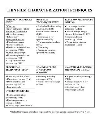
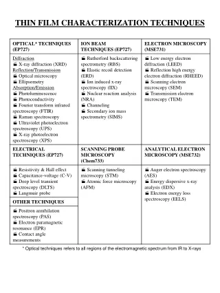
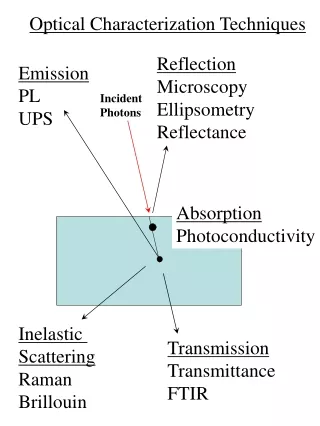
Download
1 / 45
810 likes | 1.56k Views
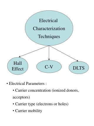
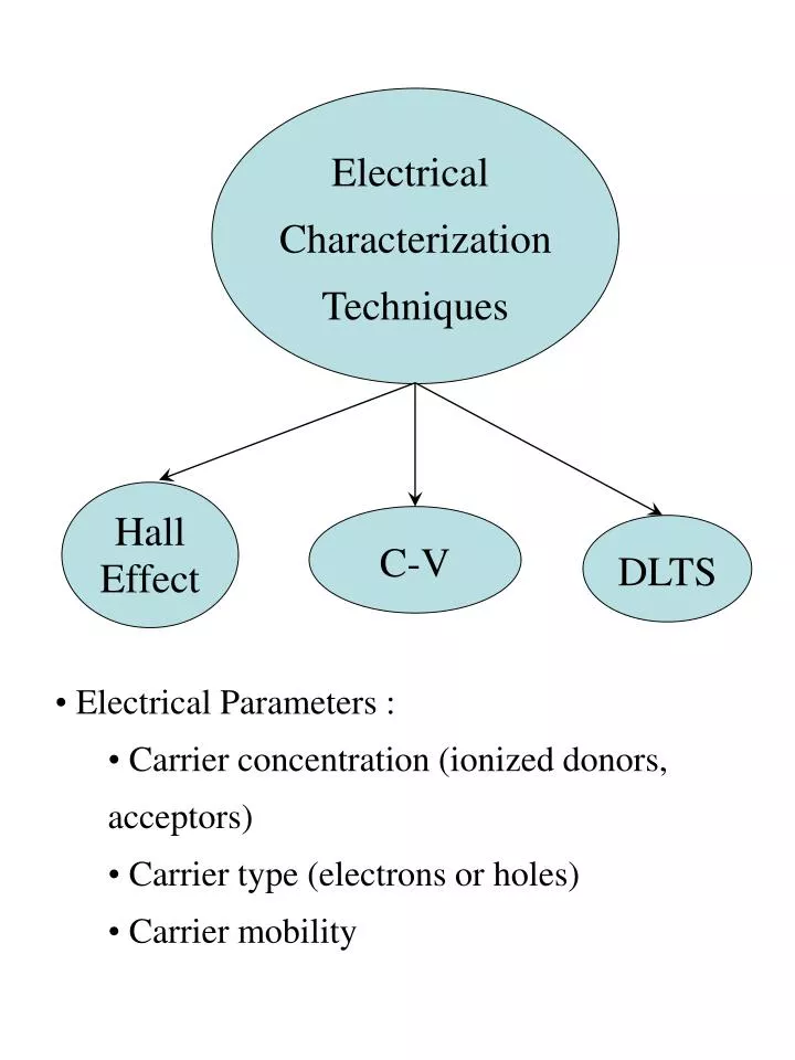
Electrical Characterization Techniques. Hall Effect. C-V. DLTS. Electrical Parameters : Carrier concentration (ionized donors, acceptors) Carrier type (electrons or holes) Carrier mobility. Derive Ohm’s law: V = IR Consider a block of material

E N D
Electrical Characterization Techniques Hall Effect C-V DLTS • Electrical Parameters : • Carrier concentration (ionized donors, acceptors) • Carrier type (electrons or holes) • Carrier mobility
Derive Ohm’s law: V = IR • Consider a block of material • What is the current, I, for an applied voltage, V ? I - + V
Total Current, I n = # electrons per unit volume v = velocity of electrons in the material # electrons in volume AL, N = nAL time to travel distance L, t = L / v I = Q/t = qN/t = q (nAL) / (L/v) = A nqv volume AL A L I - + V
Electron Velocity, v What is the electron velocity, v ? Electric field in material, E = V/L Force on an electron, F = qE Electron acceleration, a = F/m L a E I - + V
Electron Velocity, v Electrons accelerate until they collide with atoms in the material Assume electron loses all its energy (v=0) after each collision L E I - + V
Mobility • Electron velocity, v = at • ~ 10-12s • v = F t / m • = qEt / m • = (qt / m) E • = mE m = electron mobility = qt / m
Conductivity I = A nqv = A nq m E Current density, J = I / A = nqmE = sE s = conductivity = nqm = nq2t / m Resistivity, r = 1 / s
Ohm’s Law I = A nqm E = A nqm V/L Rearranging gives V = I (L/Anqm) Resistance, R = L / Anqm = L/sA = rL/A Units: [R] = W [r] = W cm [s] = (W cm)-1 [m] = cm2 / Vs
Conductivity Measurement Jx = Ix / A = Ix / tW Ex = Vx / L s = Jx / Ex = Ix L / Vx tW Ix Vx t W L A = tW • Usually use symmetric samples (L = W): • s = Ix / Vxt • Measure Ix, Vx, t Can determine s • s = nqm Can determine n if mobility is known (or vice versa) • Need another technique to determine n or m
Hall Effect : Simple Analysis • Discovered by Hall in 1879 on Au foils • Reference (review article): • D.A. Anderson and N. Apsley, “The Hall Effect in III-V Semiconductor Assessment”, Semicond. Sci. Technol. 1, 187 (1986)
Hall Effect : Simple Analysis Vx Vy Bz Bz vx t Ey W L Ix Ex A = tW Ix • Carriers experience force from : • Applied electric field, Fx = qEx • Applied magnetic field, Fy = qvxBz • Typical field ~ 0.05 - 1 Tesla = 500 - 104 Gauss • Carriers are deflected • producing an electric field, Ey = Vy / W • (Hall voltage) • Electric field builds up that counteracts magnetic field force • Sign of Hall voltage gives dominant carrier type
Hall Effect At equilibrium, qEy + qvxBz = 0 Ey = - vxBz vx = Jx / nq Jx = Ix / tW Vy t / BzIx = - (nq)-1 Ey = Vy / W Define Hall coefficient, RH = - (nq)-1 =Vy t / BzIx Measure Hall coefficient Then n = - (RHq)-1 Measure conductivity (at B=0) Then m = s / nq Or m = - RHs
Van der Pauw Technique C D B A • Gives RH, s for arbitrary sample shapes • Assumptions : • Contacts are at circumference of sample • Contacts are much smaller than sample area • Sample is uniformly thick • Sample has no holes • Sample thickness << contact spacing • References : • L.J. van der Pauw, Philips Research Reports 13, 1 (1958) • L.J. van der Pauw, Philips Research Reports 20, 220 (1961)
Van der Pauw Technique C D B A • Conductivity measurement (when B = 0) : • Apply IBC,measure VDA, define RBC-DA = VDA/IBC • Apply IAB,measure VCD, define RAB-CD = VCD/IAB • van der Pauw analysis : • r=(s)-1 = (p/ln2) t [(RBC-DA +RAB-CD)/2] F(RAB-CD /RBC-DA ) • Previous simple analysis gave : • r=(s)-1 = t Vx / Ix 4.53 correction factor
Van der Pauw Technique Correction factor, F from Schroder, Fig. 1.7, p. 15 RAB-CD / RBC-DA • Usually use symmetric samples (F ~ 1): C D B A
Van der Pauw Technique D C A B • Hall effect measurement : • Apply B perpendicular to surface • Apply IBD • Measure DRBD-AC = VAC(B) / IBD – VAC(0)/IBD • Then RH = ( t / B) DRBD-AC • Previous simple analysis gave : • RH = ( t / B ) (Vy / Ix)
Application to Thin Films thin film substrate • Want to measure n, m of thin film not substrate • Conductance of substrate must be very low compared to film • No current flow in substrate • Use semi-insulating (S.I.) substrates • S.I. substrate created by doping with an impurity producing deep traps (acceptors) • e.g., Cr in GaAs • Fe in InP
Film Thickness • What is the film thickness, t ? • Depletion layers form at surfaces and interfaces due to defects • Fermi level is pinned at EF • Chandra et al., Solid State Electronics 22, 645 (1979) • t = d – Ls- Li Substrate Film d Ls Li EF
Film Thickness • For GaAs with n ~ 1015 cm-3 • Ls ~ 1 mm, Li ~ 1 mm • Need thick films, d > 2 – 3 mm
Compensation • Conductivity and Hall effect measure net free carrier concentration • n = ND+- NA- • Or p = NA-- ND+ • Mobility can determine the compensation ratio : • q = NA- / ND+ • Walukiewicz et al., J. Appl. Phys. 51, 2659 (1980) n
Compensation compensation ratio, q = NA- / ND+ Walukiewicz et al., J. Appl. Phys. 51, 2659 (1980)
Compensation • Mobility is affected (reduced) by scattering mechanisms between the free carriers (electrons and holes) and the sample • Scattering mechanisms: • Phonons (acoustic + optical) • Impurity atoms (neutral + ionized) • Alloy disorder • Scattering from surfaces and interfaces • Defect scattering
Temperature-Dependent Hall Effect/Conductivity • Can determine scattering mechanisms by using temperature-dependent measurements At low T, ionized impurity scattering dominates At high T, phonon scattering dominates From Ibach & Luth, Fig. 12.13, p. 291
Temperature-Dependent Hall Effect/Conductivity • Can determine scattering mechanisms by using temperature-dependent measurements At low T, ionized impurity scattering dominates At high T, phonon scattering dominates From Ibach & Luth, Fig. 12.12, p. 291
Temperature-Dependent Hall Effect • Can determine donor or acceptor energy levels • n ~ exp [ – (EC – ED)/kT ] • Donors become increasingly ionized as T increases • slope of Arrhenius plot (log n vs 1/T) EC – ED
C-V • Gives n = ND+ as a function of depth • Requires a device: Schottky diode, p-n junction • e.g., apply metal contacts to semiconductor sample to form Schottky diode • Apply reverse bias voltage, V W + + + + + -eV + + + + + + + + + + + + + + + + EF
C-V • Apply small ac signal (dV~ 10 mV @ 1 MHz) on top of dc reverse bias • Depletion width varies (dW) with ac signal (dV) • Causes donor ionization over width dW • Measure capacitance change • Can determine n = ND+ W + + + + + + + -eV + + + + + + + + + + + + + + EF + + + + + -e(V+ dV) + + + + + + + + + + + + + + + EF dW
C-V C = eA/W dQ = - e ND+ A dW C = - dQ/dV = eA ND+ dW/dV • ND+ = 2 • eeA2 [ d(1/C2)/dV ] • Can determine ND+ from slope of 1/C2 versus V 1/C2 slope = 2/ [eeA2 ND+] V • Can convert voltage scale to depth scale by W = eA/C
C-V from Schroder, Fig. 2.2, p. 67
C-V • Usually assume n = ND = ND+ : • All donors become ionized • Minority carriers are neglected • All majority carriers in depletion region are removed
C-V Interface characterization (MOSFETs)
C-V • Disadvantage : • Maximum depth is limited by electrical breakdown at high reverse bias • C-V Profiling : • Can perform C-V measurement while performing a chemical etch • Reference : • T. Ambridge et al., J. Appl. Electrochem. 5, 319 (1975)
Electrochemical C-V Profiling • Replace metal contact with electrolytic solution • Destructive method
DLTS • Deep level transient spectroscopy • Reference : • D.V. Lang, J. Appl. Phys. 45, 3023 (1974)
DLTS • What are traps ? • Unwanted impurities or crystal defects • → e.g., Fe, Au in InP, GaAs • → Introduces discrete energy levels in the bandgap, usually near midgap • → Trap electrons or holes + + + + + + + + EF ET Electron traps
DLTS • Electron traps • Negative when an e- is captured • Neutral when empty • Acceptor-like • Hole traps • Positive when a hole is captured • Neutral when empty • Donor-like + + + + + + + + EF Electron traps ET
DLTS • Requires Schottky diode or p-n junction • e.g., apply metal contacts to sample to form Schottky diode • Apply reverse bias pulse and measure capacitance transient • Gives : • NT vs W • NT energy levels
W0 DLTS V C 0 C0 EF t t WV0 Transient V C -eV EF -V t CV0 t WV Steady-state V C -eV EF CV -V t t
DLTS V C CV -V t CV0 t • DC = CVNT / 2ND • Capacitance transient gives trap concentration, NT
DLTS WV0 V C -eV EF CV -V t CV0 t • Capacitance transient is characteristic of the emission of electrons from the traps: • DC(t) = DC exp (-ent) emission rate en ~ exp [ - (Ec – ET)/ kT ]
DLTS • DC(t) = DC exp (-ent) • en ~ exp [ - (Ec – ET)/ kT ] • Capacitance transient varies with temperature From Schroder, Fig. 5.12, p. 291
DLTS DC(t) = DC exp (-ent) From Schroder, Fig. 5.12, p. 291 • Define a “rate window” using two times, t1 and t2 • C(t2) – C(t1) is maximum when • (t1-t2)/ln(t1/t2) = 1 / en(T) • e.g., C(t2) – C(t1) is maximum at 260 K in above figure
DLTS • Vary the temperature and measure DC with t1 & t2 fixed • Produces peak when (t1-t2)/ln(t1/t2) = 1 / en(T) • en ~ exp [ - (Ec – ET)/ kT ] • Each kind of trap has different ET and therefore en • Produces a distinct peak for each trap • Called the DLTS spectrum From D.V. Lang, JAP 45, 3023 (1974)
DLTS • Vary the rate window • Peak moves to new position From D.V. Lang, JAP 45, 3023 (1974)
DLTS • Slope of Arrhenius plot (log en vs 1/T) gives trap energy level, ET From D.V. Lang, JAP 45, 3023 (1974)