Download
1 / 1
10 likes | 110 Views
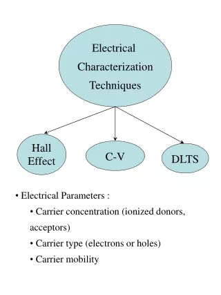
Electrical Characterization of Graphite Oxide. by Ira Jewell.

E N D
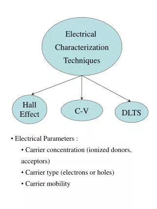
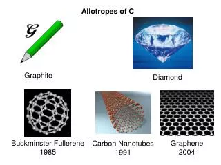
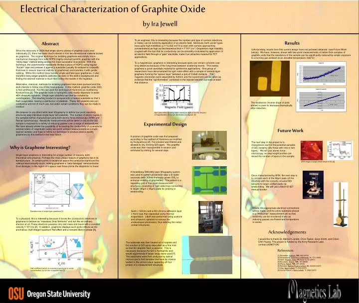
Electrical Characterization of Graphite Oxide by Ira Jewell To an engineer, this is interesting because the number and type of carriers (electrons or holes) can be tuned by application of an electric field. Moreover, both carrier types have quite high mobilities (μ≈ 10,000 cm2/V-s) even with carriers approaching concentrations as high as the theoretical limit ≈ 7*1012 cm-2.Graphene’s high mobililty, coupled with the fact that its conductivity can be smoothly modulated by application of an electric field through a “gate” electrode, make it an attractive material for FET applications. Results Abstract Unfortunately, results from this current design have not yet been obtained (see Future Work below). We have, however, shown with two-point measurements of rather thick samples of graphite oxide that the resistance of the sample can be significantly reduced by simple exposure to a forming gas ambient at an elevated temperature (300°C) Since the discovery in 2004 that single atomic planes of graphite could exist individually [1], there has been much interest in this two-dimensional material known as graphene. The original technique for isolating graphene was simply micro-mechanical cleavage from bulk HOPG (highly-oriented pyrolitic graphite) with the “sticky-tape” method being among the most successful innovations. With this technique, the experimenter repeatedly divides a piece of HOPG using regular “Scotch” tape and presses it against a substrate (usually Si oxidized to a specific thickness to ensure maximal visibility of graphenes) and transfers it with gentle rubbing. While this method does transfer single and few-layer graphenes, it also transfers many larger graphitic particles (as seen in this slide’s background) and finding the desired material is much like finding the needle in the haystack. Alternative, chemical, methods for isolating graphene have been pursued and this work intends to follow one of the most popular. In this method, graphite oxide (GO) is first synthesized. For this we used the technique of Hummers as modified by Kovtyukhova [2]. This graphite oxide is hydrophilic and readily disperses in water with ultrasonic agitation. Single-layer platelets can then be isolated by centrifugation. The resulting product is sprayed onto a heated substrate so that it flash evaporates, leaving a distribution of platelets. These GO platelets are non-conductive and not of much use, but under certain conditions they can be made to conduct. We propose to use direct-write laser lithography to define four-point resistivity structures atop individual single-layer GO platelets. The number of atomic layers in the samples will be characterized using both atomic force microscopy (AFM) and Raman spectroscopy. Resistivity measurements will be taken in situ as the GO sample is exposed to a variety of reducing gasses over a range of temperatures. We have already shown the possibility of increasing the conductivity of a sample by several orders of magnitude (using two-point contact measurements on a multi-layered sample) and hope to refine our technique to produce device-quality graphenes by this method in the near future. To a magnetician, graphene is interesting because spins can remain coherent over long distances because of the long times between scattering events. This makes graphene a good candidate material for spintronics applications. One group of researchers have demonstrated the spin valve effect with a sample of several-layer graphene forming the “spacer layer” between a pair of Cobalt contacts. The magnetic electrodes were separated by 500nm and the experiment can be taken as evidence that the “spinformation” contained in the injected electron survives at least that distance. The resistance (inverse slope of plots shown) is seen to decrease dramatically after reduction. Spin valve effect showing lower resistance state when the direction of magnetization of the two electrodes are aligned. [6] Experimental Design Future Work A solution of graphite oxide was first prepared according to the method of Hummers as modified by Kovtyukhova [2]. The solution was filtered and allowed to dry, forming GO paper. The graphite oxide was then resuspended in solution and exfoliated by stirring for several days. The next step in the project is to characterize each of the potential samples of GO, keeping only those with one or two layers. We will use atomic force microscopy, as step height profiles can reveal the number of layers in the sample. Why is Graphene Interesting? Single-layer graphene is interesting for a large number of reasons, both theoretical and practical. Perhaps the most unique feature of graphene lies in its bandstructure. At certain points in reciprocal space the conduction band and the valence band actually touch, making graphene a “zero-bandgap” semiconductor. Even stranger, in the region of k-space near these points the dispersion is linear. AFM image of single folded sheet of GO [8] A Heidelberg DWL66fs laser lithography system was used to pattern photoresist atop a Si wafer substrate (with 300nm thermally grown SiO2 to enhance visibility of graphenes). The pattern is a repeating grid of four-point measurement structures consisting of 1μm wide lines connecting to larger (90μm x 90μm) pads for probing or wirebonding. Once characterized by AFM, the next step is to connect each of the 90μm pads (of the structure with the correctly situated GO sample) to larger contact pads via wirebonding. We will use a Mech-El 827 manual bonder. Finally, the appropriate electrical connections will be made, and the entire substrate placed in a “ProboStat” measurement cell so that resistivity can be monitored in situ as reducing gasses are flowed and temperature is varied. Gold (~100nm) and a thin chrome adhesion layer (~5nm) was then deposited using thermal evaporation. Liftoff was performed using acetone and ultrasonic agitation to remove the undeveloped photoresist, thus defining the metal contact structures. Bandstructure of single-layer graphene [3] To a physicist, this is interesting because it forces the (conduction) electrons in graphene to behave as “massless Dirac fermions” and not like an ordinary electron at all. These electrons possess zero rest mass and travel with a constant velocity ≈ 106 m/s [4]. In addition, graphene displays such exotic effects as the anomalous (half-integer) quantum Hall effect and a nonzero Berry’s phase [5]. Acknowledgements I would like to thank Dr. Albrecht Jander, Chris Tasker, Sean Smith, and Chien-Chih Huang. This project is funded by the Army Research Labscontract #/280710A/ The substrate was then heated on a hotplate and the solution of GO spray deposited as a fine mist so that the droplets flash-evaporate. This is necessary because the GO is hydrophilic and would agglomerate if larger drops were used [7]. The substrates were then analyzed by optical microscope to find samples that have by chance landed in the correct place (spanning all four probes of a measurement structure) References [1] Novoselov. Science.306, 666 (2004) [2] Kovtyukhova. Chemistry of Materials. 11, 771 (1999) [3] Geim. Physics Today. 60 (Issue 8), 35 (2007) [4] Novoselov. Nature. 438, 197 (2005) [5] Zhang. Nature. 438, 201 (2005) [6] Nishioka. Applied Physics Letters. 90, 252505 (2007) [7] Gilje. Nano Letters. 7, 3394 (2007) [8] Gomez-Navarro. Nano Letters. 7, 3499 (2007) Hall coefficient (which is inversely proportional to carrier concentration) as function of applied field [1]