Download
1 / 43
980 likes | 2.15k Views
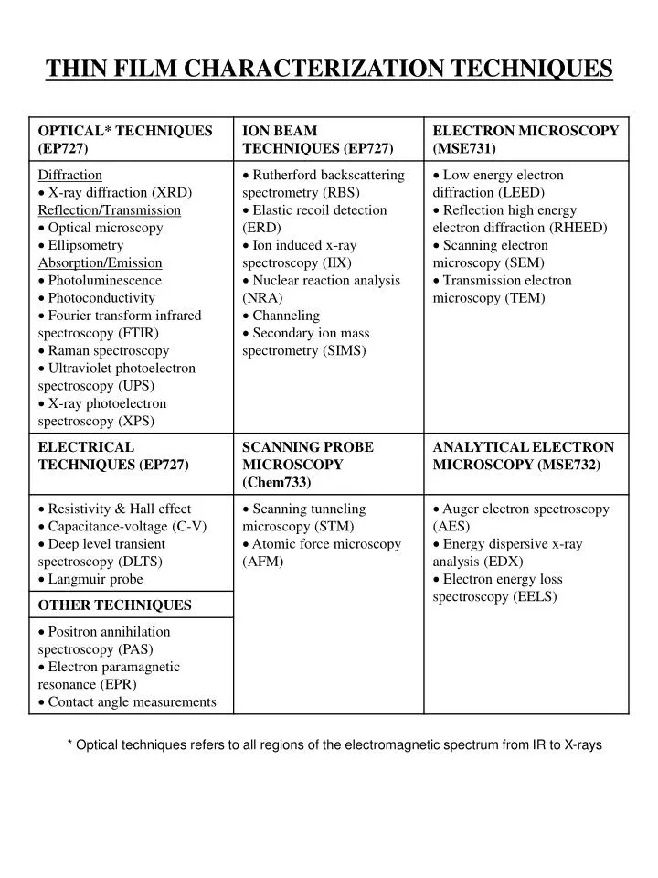
THIN FILM CHARACTERIZATION TECHNIQUES. * Optical techniques refers to all regions of the electromagnetic spectrum from IR to X-rays. THIN FILM CHARACTERIZATION TECHNIQUES. Mass, energy, or wavelength of reflected or transmitted particles are measured

E N D
THIN FILM CHARACTERIZATION TECHNIQUES * Optical techniques refers to all regions of the electromagnetic spectrum from IR to X-rays
THIN FILM CHARACTERIZATION TECHNIQUES • Mass, energy, or wavelength of reflected or transmitted particles are measured • Used to determine film structure, composition, thickness, etc. Incident electrons, ions, or photons Reflected or emitted particles Sample Transmitted particles
Film Structure Direct Imaging Diffraction (electrons, x-rays) SPM LEED RHEED XRD Electron Microscopy
Crystal Structures • 14 Bravais lattices From Kittel, Fig. 11, p. 14
Crystal Structures From Kittel, Table 1, p. 15 From Kittel, Fig. 12, p. 15
Miller Indices for Crystal Planes c/l b/k a/h • Lattice vectors are a, b, c • (hkl) are the Miller indices for the plane with intercepts a/h, b/k, c/l • Spacing between planes with Miller indices (hkl) is denoted ahkl • For cubic crystal with lattice constant a, • ahkl = a / (h2 + k2 + l2)½
Diffraction • Incident particles (electrons, x-rays) treated as a plane wave (large distances, R;far-field orFraunhofer diffraction condition) • Amplitude of incident wave at point P in crystal (polar notation): • ψP(r,t) = A e i k·(R+r) – iwt phase Incident wave, k = 2p/l R O r crystal P
Diffraction • Amplitude at detector D due to scattering from point P : • ψD,P(r,t) = ψP(r,t)r(r)e i k´·(R´-r) R´- r scattering density = electron probability density In structural analysis we are interested in determining r(r) S D R R´ R´ - r O r crystal P
Diffraction ψD,P(r,t) = ψP(r,t)r(r)e i k´·(R´-r) R´- r w´ = w Forced oscillation; elastic scattering S D R R´ R´ - r O r crystal P
Diffraction • For large R´ (far-field or Fraunhofer diffraction condition): • ψD,P(r,t) = ψP(r,t)r(r)e i k´·(R´-r) • =[(A/R´)e-iwt ei(k·R+k´·R´)]r(r)ei(k-k´)·r R´ S D R R´ R´ - r O r crystal P
Diffraction ψD,P(r) ~ r(r) ei(k-k´)·r ~r(r)e -i K·r scattering vector, K = k´ - k S D R R´ R´ - r O r crystal P
Diffraction • Total amplitude of wave scattered from crystal: • ψ~∫ r(r)e - i K·r dr • Amplitude is the Fourier transform of the scattering density • Total intensity: • I ~∫ r(r)e - i K·r dr 2 • phase problem : we measure intensity not amplitude • must determine structure by comparison of experimental diffraction pattern with simulated pattern from model structure V
Diffraction • Incident wave is elastically scattered by atomic array • Constructive interference occurs in specific directions Incident wave, k = 2p/l Scattered Waves k' = 2p/l a
Diffraction • Same physics as diffraction grating slit N ... Optical path length difference q q ... P slit 1
Diffraction • Constructive interference occurs when: • Path length difference = ml • 2ahkl sinq = ml • (Bragg condition) • m = diffraction order = 1, 2, 3, … • q’s that satisfy the Bragg condition are called Bragg angles, qb k' k k' k q A ahkl r B
Diffraction Note : q defined relative to surface plane, not the surface normal (as in optics) k' k k' k q A ahkl r B
Diffraction • Phase difference between plane waves reflected from atoms such as A and B is • Df = (k' – k)•r = K•r • Constructive interference occurs when • Df = 2p • or • K = (2p/ahkl) n • (Laue condition) n = unit vector along surface normal k' k k' k q A ahkl r B
k' Diffraction • K = (2p / ahkl) n • (Laue condition) • ghkl = (2p/ahkl)n is called a reciprocal lattice vector • ghkl is normal to the hkl set of crystal planes • K = ghkl • (Laue condition) ghkl =(2p / ahkl) n qb qb k qb
Miller Indices ghkl c/l b/k a/h • Lattice vectors are a, b, c • Reciprocal lattice vectors are a*, b*, c* • ghkl = (ha* + kb* + lc*) is orthogonal to hkl plane; h, k, l are integers
Diffraction • The set of all ghkl points is called reciprocal space • ghkl defines a point in reciprocal space for each set of crystal planes in real space with spacing ahkl ghkl Origin, O
Diffraction • Superimpose Laue condition on reciprocal space (hkl) k' ghkl 2qb k O
Diffraction • Sphere of radius k= 2p/l is called the Ewald sphere C k = 2p/l O
Diffraction • K = ghkl (Laue condition) • Laue condition is satisfied by any reciprocal lattice point that intersects the Ewald sphere (hkl) k' ghkl C 2qb k O
Diffraction Crystal Crystal = Unit cell + Basis (e.g., fcc)
Diffraction r = rm + rn + ra position vector from centre of charge distribution within each atom position of mth unit cell position of nth atom in each unit cell ra rn rm O
Diffraction • Total scattering amplitude is • ψ ~ ∫r(r) e -i K·(rm + rn + ra) dr • = S [ ∫ rn(ra) e-iK·ra dra] e-iK·(rm+rn) • = S fne-iK·rnS e-iK·rm phase difference m,n A atomic scattering factor, fn Tabulated for each element n m structure factor, F shape factor
Diffraction • Amplitude of wave scattered from a single unit cell: • F = Σ fn exp -iK·rn position of atom n in unit cell Structure factor n phase difference scattering factor from atom n summation over n atoms in unit cell Assumes electrons only scatter once (kinematic approximation)
Diffraction • Amplitude of wave diffracted from unit cell at Bragg angle (Laue condition): • F = Σ fn exp -i ghkl·rn • Diffraction spots will appear when F ≠ 0 • F (the diffraction pattern) is the Fourier transform of fn (the crystal structure) F = Σ fn exp -i K·rn n n
Diffraction • e.g., fcc lattice • 4 atoms per unit cell (one at each lattice point) at • r1 = (0a + 0b + 0c) • r2 = (½a + ½b + 0c) • r3 = (½a + 0b + ½c) • r4 = (0a + ½b + ½c) c 4 3 b 2 1 a
Diffraction F = Σ fn exp -i ghkl·rn ghkl = (ha*+ kb*+ lc*) r1 = (0a + 0b + 0c) r2 = (½a + ½b + 0c) r3 = (½a + 0b + ½c) r4 = (0a + ½b + ½c) F = f [ 1 + e-ip(h+k) + e-ip(h+l) + e-ip(k+l) ] 0 if h, k, l are mixed (even & odd) integers 4f if h, k, l are unmixed (all even or all odd) e.g., (400) → F = 4f e.g., (211) → F = 0 n F =
Diffraction • F = 0 are called forbidden reflections • Not all reciprocal lattice points satisfying the Laue condition will result in a diffraction spot (hkl) k' ghkl C qb k O
Diffraction • e.g., bcc lattice • 2 atoms per unit cell at • r1 = (0a + 0b + 0c) • r2 = (½a + ½b + ½c) • F = f [1 + e-ip(h+k+l) ] • 0 if h+k+l is odd • 2f if h+k+l is even F = c 2 b 1 a
Diffraction • A unit cell may have a basis with different atoms • e.g., bcc structure for NiAl • rNi = (0a + 0b + 0c) • rAl = (½a + ½b + ½c) • F = fNi + fAle-ip(h+k+l) • fNi – fAl if h+k+l is odd • fNi + fAl if h+k+l is even • Weak spots appear called superlattice peaks or spots • The more intense peaks are called the fundamentals F =
Diffraction • The symmetry and forbidden reflections of the diffraction pattern can be used to determine the crystal structure
Diffraction • Total scattering amplitude near the Bragg angle is • ψ = Σ fn exp -i(ghkl + s)·(rn + rm) Position of atom n in unit cell n,m Small deviation from Laue condition Position of mth unit cell in crystal Sum over all unit cells, m, in sample and all atoms, n, per unit cell
Diffraction s k' ghkl C k O
Diffraction • Total scattering amplitude near the Bragg angle is • ψ = Σ fi exp -i(ghkl+s)·(rn + rm) • = Σ[Σ fnexp -i(gkhl+s)·rn]exp -i(ghkl+s)·rm • = F Σ exp -i(ghkl·rm) exp -i(s·rm) n,m m n = structure factor, F,since s << ghkl m = 1 since ghkl = (ha* + kb* + lc*) rm = (n1a + n2b + n3c) where h, k, l, n1, n2, n3 = integer ghkl·rm = 2p (n1h + n2k + n3l)
Diffraction • ψ = F Σ exp -i (s·rm) • For rectangular crystal with dimensions xa, yb, zc : • ψ = F sin(½sxxa) sin(½syyb) sin(½szzc) • ½sxxa ½sy yb ½sz zc • V = sample volume = xaybzc • For a thin film z << x, y • Assume sx = sy = 0 • ψ = F sin (½szzc) • V ½sz m shape factor
Diffraction • ψ = F sin (½szzc) • V ½sz • Now zc = film thickness, t • ψ = F sin (½szt) • V ½sz • Intensity of diffracted wave is : • I = ψ2 = (F/V)2 [( sin(½szt) )/(½sz)]2 • = (tF/V)2 sinc2(½szt)
Diffraction I = ψ2 = (tF/V)2 sinc2(½szt) I / (tF/V)2 ½szt -3p -2p -p 0 p 2p 3p • I = 0 when x = ±p • width, 2p = 2 (½szt) = szt • sz = 2p / t
Diffraction • Due to finite thickness of the film, each reciprocal lattice point may be considered as streaks with length 2p/t 2p/t k' ghkl C k O
Diffraction • The thinner the film the greater the “streaking” • Lattice points become lattice rods for very thin films (monolayers) from Ohring, Fig. 7-27, p. 346
Diffraction From Tom Ryan, MRS short course (1990)