Download
1 / 51
540 likes | 684 Views
Sequential Logic. Introduction to Computer Yung-Yu Chuang. with slides by Sedgewick & Wayne ( introcs.cs.princeton.edu ), Nisan & Schocken ( www.nand2tetris.org ) and Harris & Harris (DDCA). ALU combinational. Memory state. Review of Combinational Circuits. Combinational circuits.

E N D
Sequential Logic Introduction to Computer Yung-Yu Chuang with slides by Sedgewick & Wayne (introcs.cs.princeton.edu), Nisan & Schocken (www.nand2tetris.org) and Harris & Harris (DDCA)
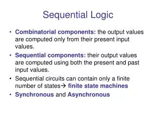
ALU combinational Memory state Review of Combinational Circuits • Combinational circuits. • Basic abstraction = switch. • In principle, can build TOY computer with a combinational circuit. • 255 16 = 4,080 inputs 24080 rows in truth table! • no simple pattern • each circuit element used at most once • Sequential circuits. Reuse circuit elements by storing bits in "memory."
Combinational vs. Sequential Circuits • Combinational circuits. • Output determined solely by inputs. • Can draw with no loops. • Ex: majority, adder, ALU. • Sequential circuits. • Output determined by inputs and previous outputs. • Ex: memory, program counter, CPU.
Flip-Flop • Flip-flop • A small and useful sequential circuit • Abstraction that remembers one bit • Basis of important computer components for • register • memory • counter • There are several flavors
Q=S+RQ S-R flip flop
Relay-based flip-flop Ex. Simplest feedback loop. • Two relays A and B, both connectedto power, each blocked by the other. • State determined by whichever switches first. The state is latched. • Stable. output1 input1 input2 output2
Q=R(S+Q) SR Flip Flop • SR flip flop. Two cross-coupled NOR gates. S R Q
Flip-Flop • Flip-flop. • A way to control the feedback loop. • Abstraction that "remembers" one bit. • Basic building block for memory and registers. • Caveat. Need to deal with switching delay.
Truth Table and Timing Diagram SR Flip Flop Truth Table • Truth table. • Values vary over time. • S(t), R(t), Q(t) denote value at time t. • Sample timing diagram for SR flip-flop. S(t) R(t) Q(t) Q(t+) 0 0 0 0 0 0 1 1 0 1 0 0 0 1 1 0 1 0 0 1 1 0 1 1 1 1 0 1 1 1 e e 1 Q 0 1 R 0 1 S 0 time
Clock • Clock. • Fundamental abstraction: regular on-off pulse. • on: fetch phase • off: execute phase • External analog device. • Synchronizes operations of different circuit elements. • Requirement: clock cycle longer than max switching time. cycle time on Clock off
How much does it Hert? • Frequency is inverse of cycle time. • Expressed in hertz. • Frequency of 1 Hz means that there is 1 cycle per second. • 1 kilohertz (kHz) means 1000 cycles/sec. • 1 megahertz (MHz) means 1 million cycles/sec. • 1 gigahertz (GHz) means 1 billion cycles/sec. • 1 terahertz (THz) means 1 trillion cycles/sec. Heinrich Rudolf Hertz(1857-1894)
Two-input multiplexer Multiplexer • When s=0, return x; otherwise, return y. • Example: (Y S) (X S)
4-to-1 multiplexer 4MUX x0 x1 z x2 x3 s0 s1
x0 2MUX x1 2MUX z x2 2MUX x3 s0 s1 4-to-1 multiplexer 4MUX x0 x1 z x2 x3 s0 s1
8-to-1 Multiplexer • 2N-to-1 multiplexer • N select inputs, 2N data inputs, 1 output • Copies “selected” data input bit to output
8-to-1 Multiplexer • 2N-to-1 multiplexer • N select inputs, 2N data inputs, 1 output • Copies “selected” data input bit to output
4-Wide 2-to-1 Multiplexer • Goal: select from one of two 4-bit buses
4-Wide 2-to-1 Multiplexer • Goal: select from one of two 4-bit buses • Implemented by layering 4 2-to-1 multiplexer
k-Wide n-to-1 Multiplexer • Goal: select from one of n k-bit buses • Implemented by layering k n-to-1 multiplexer
Memory Overview • Computers and TOY have several memory components. • Program counter. • Registers. • Main memory. • Implementation. Use one flip-flop for each bit of memory. • Access. Memory components have different access mechanisms. • Organization. Need mechanism to manipulate groups of related bits. TOY has 16 bit words,8 bit memory addresses, and4 bit register names.
Register Bit • Register bit. Extend a flip-flop to allow easy access to values.
Register Bit • Register bit. Extend a flip-flop to allow easy access to values. D W DW DW
Memory Bit: Interface • Memory bit. Extend a flip-flop to allow easy access to values. [ TOY PC, IR ] [ TOY main memory ] [ TOY registers ]
Memory Bit: Switch Level Implementation • Memory bit. Extend a flip-flop to allow easy access to values. [ TOY PC, IR ] [ TOY main memory ] [ TOY registers ]
Processor Register • Processor register. • Stores k bits. • Register contents always available on output bus. • If enable write is asserted, k input bits get copied into register. • Ex 1. TOY program counter (PC) holds 8-bit address. • Ex 2. TOY instruction register (IR) holds 16-bit current instruction.
Processor Register • Processor register. • Stores k bits. • Register contents always available on output bus. • If enable write is asserted, k input bits get copied into register. • Ex 1. TOY program counter (PC) holds 8-bit address. • Ex 2. TOY instruction register (IR) holds 16-bit current instruction.
Processor Register • Processor register. • Stores k bits. • Register contents always available on output bus. • If enable write is asserted, k input bits get copied into register. • Ex 1. TOY program counter (PC) holds 8-bit address. • Ex 2. TOY instruction register (IR) holds 16-bit current instruction.
Memory Bank • Memory bank. • Bank of n registers; each stores k bits. • Read and write information to one of n registers. • Address inputs specify which one. • Addressed bits always appear on output. • If write enabled, k input bits are copied into addressed register. • Ex 1. TOY main memory. • 256-by-16 memory bank. • Ex 2. TOY registers. • 16-by-16 memory bank. • Two output buses. log2n address bits needed (four 6-bit words) 6-bit input bus 2-bit address 6-bit output bus
Memory: Interface (four 6-bit words)
Memory: Switch Level Implementation (four 6-bit words)
Summary • Sequential circuits add "state" to digital hardware. • Flip-flop. [represents 1 bit] • TOY word. [16 flip-flops] • TOY registers. [16 words] • TOY main memory. [256 words] • Modern technologies for registers and main memory are different. • Few registers, easily accessible, high cost per bit. • Huge main memories, less accessible, low cost per bit. • Drastic evolution of technology over time. • Next. Build a complete TOY computer.
The Clock • In our jargon, a clock cycle = tick-phase (low), followed by atock-phase (high) • In real hardware, the clock is implemented by an oscillator • In our hardware simulator, clock cycles can be simulated either • Manually, by the user, or • “Automatically,” by a test script.
in DFF out out(t) = in(t-1) Flip-flop • A fundamental state-keeping device • For now, let us not worry about the DFF implementation • Memory devices are made from numerous flip-flops,all regulated by the same master clock signal • Notational convention:
in out DFF out(t) = out(t-1) ? out(t) = in(t-1) ? Won’twork 1-bit register (we call it “Bit”) Objective: build a storage unit that can: • Change its state to a given input • Maintain its state over time (until changed)
Interface Implementation Bit register (cont.) • Load bit • Read logic • Write logic
Multi-bit register • Register’s width: a trivial parameter • Read logic • Write logic
Aside: Hardware Simulation Relevant topics from the HW simulator tutorial: • Clocked chips: When a clocked chip is loaded into the simulator, the clock icon is enabled, allowing clock control • Built-in chips: • feature a standard HDL interface yet a Java implementation • Provide behavioral simulation services • May feature GUI effects (at the simulator level only).
Random Access Memory (RAM) • Read logic • Write logic.
RAM anatomy Recursive ascent
Counter Needed: a storage device that can: (a) set its state to some base value (b) increment the state in every clock cycle (c) maintain its state (stop incrementing) over clock cycles (d) reset its state • Typical function: program counter • Implementation: register chip + some combinational logic. If reset(t-1) then out(t)=0 else if load(t-1) then out(t)=in(t-1) else if inc(t-1) then out(t)=out(t-1)+1 else out(t)=out(t-1)
Time matters Implications: • Challenge: propagation delays • Solution: clock synchronization • Cycle length and processing speed. • During a tick-tock cycle, the internal states of all the clocked chips are allowed to change, but their outputs are “latched” • At the beginning of the next cycle, the outputs of all the clocked chips in the architecture commit to the new values.