Download
1 / 44
440 likes | 599 Views
CSE 30321 MIPS Single Cycle Dataflow. The goals of this lecture are…. …to show how ISAs map to real HW and affect the organization of processing logic… …and to set up a discussion of pipelining + other principles of modern processing…. The organization of a computer. Von Neumann Model:

E N D
The goals of this lecture are… • …to show how ISAs map to real HW and affect the organization of processing logic… • …and to set up a discussion of pipelining + other principles of modern processing…
The organization of a computer • Von Neumann Model: • Stored-program machine instructions are represented as numbers • Programs can be stored in memory to be read/written just like numbers. Compiler Today we’ll talk about these things Control Input Memory Datapath Output Processor
Functions of Each Component • Datapath: performs data manipulation operations • arithmetic logic unit (ALU) • floating point unit (FPU) • Control: directs operation of other components • finite state machines • micro-programming • Memory: stores instructions and data • random access v.s. sequential access • volatile v.s. non-volatile • RAMs (SRAM, DRAM), ROMs (PROM, EEPROM), disk • tradeoff between speed and cost/bit • Input/Output and I/O devices: interface to the environment • mouse, keyboard, display, device drivers
The Performance Perspective • Performance of a machine determined by • Instruction count, clock cycles per instruction, clock cycle time • Processor design (datapath and control) determines: • Clock cycles per instruction • Clock cycle time • We will discuss a simplified MIPS implementation
Review of Design Steps • Instruction Set Architecture => RTL representation • RTL representation => • Datapath components • Datapath interconnects • Datapath components => Control signals • Control signals => Control logic • Writing RTL: How many states (cycles) should an instruction take? • CPI • Datapath component sharing
31 26 25 21 20 16 15 11 10 6 5 0 funct (6) op (6) rs (5) rt (5) rd (5) shamt (5) 31 26 25 21 20 16 15 0 Op (6) rs (5) rt (5) Address/Immediate value (16) 31 26 25 0 Op (6) Target address (26) MIPS Instruction Formats • All MIPS instructions are 32 bits (4 bytes) long. • R-type: • I-Type: • J-type
Let’s talk about this generally on the board first… • Let’s just look at our instruction formats and “derive” a simple datapath • (we need to make all of these instruction formats “work”)
The MIPS Subset • To simplify things a bit we’ll just look at a few instructions: • memory-reference: lw, sw • arithmetic-logical: add, sub, and, or, slt • branching: beq, j • Organizational overview: • fetch an instruction based on the content of PC • decode the instruction • fetch operands • (read one or two registers) • execute • (effective address calculation/arithmetic-logical operations/comparison) • store result • (write to memory / write to register / update PC) At simplest level, this is how Von Neumann, RISC model works
What we’ll do… • …look at instruction encodings… • …look at datapath development… • …discuss how we generate the control signals to make the datapath elements work…
Clk Clk Clk Clk Implementation Overview simplest view of Von Neumann, RISC mP • Abstract / Simplified View: • 2 types of signals: data and control • Clocking strategy: All storage elements clocked by same clock edge. Data Address PC Ra Instruction Address Rb A L U Instruction Memory Register File Rw Data Memory Data
Review of Design Steps • Instruction set Architecture => RTL representation • RTL representation => • Datapath components • Datapath interconnects • Datapath components => Control signals • Control signals => Control logic • Writing RTL: How many states (cycles) should an instruction take? • CPI • Datapath component sharing i.e. PC PC + 4 (or $4 $3 + $2) need these to do need these to do need these to do
PC instr. fetch & execute Single Cycle Implementation • Each instruction takes one cycle to complete. • We wait for everything to settle down, and the right thing to be done • ALU might not produce “right answer” right away • (why?) • we use write signals along with clock to determine when to write • Cycle time determined by length of the longest path
Clk Instruction Fetch Unit • Fetch the instruction: mem[PC] , • Update the program counter: • sequential code: PC <- PC+4 • branch and jump: PC <- “something else” PC Next Addr Logic Address Instruction Word 32 Instruction Memory
31 26 25 21 20 16 15 11 10 6 5 0 funct (6) op (6) rs (5) rt (5) rd (5) shamt (5) Let’s say we want to fetch……an R-type instruction (arithmetic) • Instruction format: • RTL: • Instruction fetch: mem[PC] • ALU operation: reg[rd] <- reg[rs] op reg[rt] • Go to next instruction: Pc <- PC+ 4 • Ra, Rb and Rw are from instruction’s rs, rt, rd fields. • Actual ALU operation and register write should occur after decoding the instruction.
Register timing: Register can always be read. Register write only happens when RegWr is set to high and at the falling edge of the clock Clk Datapath for R-Type Instructions ALUctr RegWr 5 Ra 32 32-bit Registers rs BusA 32 5 Rb rt ALU 5 Rw rd BusB 32 BusW 32
31 26 25 21 20 16 15 0 Op (6) rs (5) rt (5) Address/Immediate value (16) I-Type Arithmetic/Logic Instructions • Instruction format: • RTL for arithmetic operations: e.g., ADDI • Instruction fetch: mem[PC] • Add operation: reg[rt] <- reg[rs] + SignExt(imm16) • Go to next instruction: Pc <- PC+ 4 • Also, immediate instructions
Clk MUX MUX Datapath for I-Type A/L Instructions note that we reuse ALU… ALUctr RegWr 5 Ra 32 32-bit Registers rs BusA 32 5 Rb rt ALU Rw BusB 32 5 32 BusW 32 RegDst Extender ALUSrc 16 must “zero out” 1st 16 bits… rd rt imm16 In MIPS, destination registers are in different places in opcode therefore we need a mux BusW 32
31 26 25 21 20 16 15 0 Op (6) rs (5) rt (5) Address/Immediate value (16) I-Type Load/Store Instructions • Instruction format: • RTL for load/store operations: e.g., LW • Instruction fetch: mem[PC] • Compute memory address: Addr <- reg[rs] + SignExt(imm16) • Load data into register: reg[rt] <- mem[Addr] • Go to next instruction: Pc <- PC+ 4 • How about store? same thing, just skip 3rd step (mem[addr] reg[rs])
RegWr ALUctr 5 Ra 32 32-bit Registers rs BusA 32 5 Rb rt ALU Rw BusB 32 5 MUX 32 Clk Clk ALUSrc MUX RegDst Extender MemWr 16 rt rd Addr Data Memory WrEn imm16 32 DataIn Datapath for Load/Store Instructions need a control signal address input 32 bits of data
31 26 25 21 20 16 15 0 Op (6) rs (5) rt (5) Address/Immediate value (16) I-Type Branch Instructions • Instruction format: • RTL for branch operations: e.g., BEQ • Instruction fetch: mem[PC] • Compute conditon: Cond <- reg[rs] - reg[rt] • Calculate the next instruction’s address: if (Cond eq 0) then PC <- PC+ 4 + (SignExd(imm16) x 4) else ?
Clk Clk Datapath for Branch Instructions PC Next Addr Logic To Instruction Mem RegWr ALUctr 5 Ra 32 32-bit Registers rs BusA 32 5 Rb rt ALU Rw BusB 32 5 MUX we’ll define this next; (will need PC, zero test condition from ALU) 32 Zero ALUSrc MUX RegDst Extender 16 rt rd imm16
Clk Next Address Logic contains PC + 4 (why 30? – subtlety – see Chapter 5 in your text) “1” PC CarryIn 30 ADD Instruction Memory 30 May not want to change PC if BEQ condition not met (implicitly says: “this stuff happens anyway so we have to be sure we don’t change things we don’t want to change”) “0” MUX 30 SignExt if branch instruction AND 0, can automatically generate control signal 16 Zero Branch imm16 When does the correct new PC become available? Can we do better?
31 26 25 0 Op (6) Target address (26) J-Type Jump Instructions • Instruction format: • RTL operations: e.g., BEQ • Instruction fetch: mem[PC] • Set up PC: PC <- ((PC+ 4)<31:29> CONCAT(target<25:0>) x 4
Clk MUX MUX Instruction Fetch Unit Use: New address in jump instruction OR use 4 MSB of PC (why PC<31:28> – subtlety – see Page 383 in your text) PC<31:28> Instruction<25:0> “1” PC CarryIn Jump 30 ADD 30 “0” 30 Instruction Memory SignExt 16 Branch Zero imm16
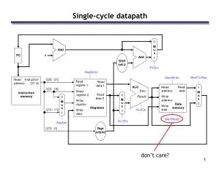
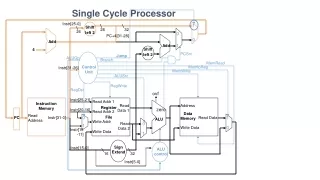
M u x A L U A d d r e s u l t S h i f t l e f R e g i s t e r s R e a d R e a d r e g i s t e r 1 P C R e a d a d d r e s s R e a d d a t a 1 r e g i s t e r 2 I n s t r u c t i o n W r i t e R e a d r e g i s t e r d a t a 2 I n s t r u c t i o n W r i t e m e m o r y d a t a 3 2 1 6 A Single Cycle Datapath P C S r c A d d 4 t 2 ALUctr 3 i M e m W r i t e A L U S r c M e m t o R e g i Z e r o A L U A L U R e a d A d d r e s s r e s u l t M d a t a M u u x D a t a x m e m o r y W r i t e R e g W r i t e d a t a S i g n M e m R e a d e x t e n d Add Jump.
Let’s trace a few instructions • For example… • Add $5, $6, $7 • SW 0($9), $10 • Sub $1, $2, $3 • LW $11, 0($12)
Control Logic (I.e. now, we need to make the HW do what we want it to do - add, subtract, etc. - when we want it to…)
The HW needed, plus control Single cycle MIPS machine When we talk about control, we talk about these blocks
Implementing Control • Implementation Steps: • Identify control inputs and control output (control words) • Make a control signal table for each cycle • Derive control logic from the control table • Do we need a FSM here? • Control outputs: • RegDst • MemtoReg • RegWrite • MemRead • MemWrite • ALUSrc • ALUctr • Branch • Jump Control input Control Path Data Path • Control inputs: • Opcode (5 bits) • Func (6 bits) Control output
Implementing Control • Implementation Steps: • Identify control inputs and control outputs • Make a control signal table for each cycle • Derive control logic from the control table • This logic can take on many forms: combinationallogic, ROMs, microcode, or combinations…
Step 1: Idenitfy inputs & outputs these are columns these are rows Single Cycle Control Input/Output • Control Inputs: • Opcode (6 bits) • How about R-type instructions? • Control Outputs: • RegDst • ALUSrc • MemtoReg • RegWrite • MemRead • MemWrite • Branch • Jump • ALUctr Step 2: Make a control signal table for each cycle
Control Signal Table (inputs) R-type (outputs)
For MIPS, we have to build a Main Control Block and an ALU Control Block The HW needed, plus control Single cycle MIPS machine
Use OP field to generate ALUOp (encoding) Control signal fed to ALU control block Use Func field and ALUOp to generate ALUctr (decoding) Specifically sets 3 ALU control signals B-Invert, Carry-in, operation Our 2 blocks of control logic Main control, ALU control Func ALUctr OP ALU Control Main Control 6 ALUOp 3 6 2 (opcode) ALU Other cnt. signals
Func ALUctr OP ALU Control Main Control 6 ALUOp 3 6 2 ALU Outputs of main control, become inputs to ALU control We have 8 bits of input to our ALU control block; we need 3 bits of output… Main control, ALU control Or in other words… 00 = ALU performs add 01 = ALU performs sub 10 = ALU does what function code says
Outputs Inputs • We have these inputs… ALUOp Funct field ALUctr func<5:0> ALUOp1 ALUOp0 F5 F4 F3 F2 F1 F0 36 (and) = 1 0 0 1 0 0 37 (or) = 1 0 0 1 0 1 32 (add) = 1 0 0 0 0 0 34 (sub) = 1 0 0 0 1 0 42 (slt) = 1 0 1 0 1 0 lw/sw 010 (add) 0 0 X X X X X X beq 110 (sub) 0 1 X X X X X X 010 (add) 1 X X X 0 0 0 0 110 (sub) 1 X X X 0 0 1 0 R-type 000 (and) 1 X X X 0 1 0 0 001 (or) can ignore these (they’re the same for all…) 1 X X X 0 1 0 1 111 (slt) 1 X X X 1 0 1 0 Generating ALUctr • We want these outputs: and - 00 or - 01 mux adder - 10 ALUctr<2> = B-negate (C-in & B-invert) ALUctr<1> = Select ALU Output ALUctr<0> = Select ALU Output Invert B and C-in must be a 1 for subtract less - 11
and and or or or Outputs Inputs ALUOp Funct field ALUctr ALUOp1 ALUOp0 F5 F4 F3 F2 F1 F0 lw/sw 010 (add) 0 0 X X X X X X beq 110 (sub) 0 1 X X X X X X 010 (add) 1 X X X 0 0 0 0 110 (sub) 1 X X X 0 0 1 0 R-type 000 (and) 1 X X X 0 1 0 0 001 (or) 1 X X X 0 1 0 1 111 (slt) 1 X X X 1 0 1 0 The Logic This table is used to generate the actual Boolean logic gates that produce ALUctr. Could generate gates by hand, often done w/SW. (ALUOp) X/1 ALUOp0 ALUctr<2> ALUOp1 1/0 0/X 1/1 F3 1/0 ALUctr (func<5:0>) 110/110 ALUctr<1> F2 0/X 1/1 Ex: ALUctr<2> (SUB/BEQ) ALUctr<0> F1 1/X 0/0 0/0 F0 0/X 0/X
Recall… Single cycle MIPS machine Recall, for MIPS, we have to build a Main Control Block and an ALU Control Block
and and or or or (ALUOp) ALUOp0 ALUctr<2> ALUOp1 F3 (func<5:0>) ALUctr ALUctr<1> F2 ALUctr<0> F1 F0 Well, here’s what we did… Single cycle MIPS machine We came up with the information to generate this logic which would fit here in the datapath.
(and again, remember, realistically logic, ISAs, insturction types, etc. would be much more complex) (we’d also have to route all signals too…which may affect how we’d like to organzie processing logic)
Single-Cycle Implementation • Single-cycle, fixed-length clock: • CPI = 1 • Clock cycle = propagation delay of the longest datapath operations among all instruction types • Easy to implement • Single-cycle, variable-length clock: • CPI = 1 • Clock cycle = (%(type-i instructions) * propagation delay of the type “i” instruction datapath operations) • Better than the previous, but impractical to implement • Disadvantages: • What if we have floating-point operations? • How about component usage?
Multiple Cycle Alternative • Break an instruction into smaller steps • Execute each step in one cycle. • Execution sequence: • Balance amount of work to be done • Restrict each cycle to use only one major functional unit • At the end of a cycle • Store values for use in later cycles, why? • Introduce additional “internal” registers • The advantages: • Cycle time much shorter • Diff. inst. take different # of cycles to complete • Functional unit used more than once per instruction