Download
1 / 25
260 likes | 499 Views
CSE 675.02: Introduction to Computer Architecture. Designing MIPS Processor (Single-Cycle) Presentation G. Slides by Gojko Babi ć. Introduction. We're now ready to look at an implementation of the system that includes MIPS processor and memory.

E N D
CSE 675.02: Introduction to Computer Architecture Designing MIPS Processor(Single-Cycle)Presentation G Slides by Gojko Babić
Introduction • We're now ready to look at an implementation of the system that includes MIPS processor and memory. • The design will include support for execution of only: • memory-reference instructions: lw & sw, • arithmetic-logical instructions: add, sub, and, or, slt & nor, • control flow instructions: beq & j, • exception handling: illegal instruction & overflow. • But that design will provide us with principles, so many more instructions could be easily added such as: addu,lb, lbu, lui, addi, adiu, sltu, slti, andi, ori, xor, xori, jal, jr, jalr, bne, beqz, bgtz, bltz, nop, mfhi, mflo, mfepc, mfco, lwc1, swc1, etc. Presentation G
Single Cycle Design • We shall first design a simpler processor that executes each instruction in only one clock cycle time. • This is not efficient from performance point of view, since: • a clock cycle time (i.e. clock rate) must be chosen such that the longest instruction can be executed in one clock cycle and • that makes shorter instructions execute in one unnecessary long cycle. • Additionally, no resource in the design may be used more than once per instruction, thus some resources will be duplicated. • Because of that, the singe cycle design will require: • two memories (instruction and data), • two additional adders. Presentation G
M e m W r i t e A L U c o n t r o l 4 32 32 32 32 32 P C R e a d A d d r e s s Z e r o d a t a 32 A L U A L U 32 r e s u l t 32 D a t a W r i t e m e m o r y d a t a a . P r o g r a m c o u n t e r M e m R e a d c . A L U e . D a t a m e m o r y u n i t 5 32 R e a d 32 MemRead=1 MemWrite =0 Shift Left 2 32 3 2 r e g i s t e r 1 R e a d d a t a 1 5 32 R e g i s t e r R e a d r e g i s t e r 2 n u m b e r s A d d S u m R e g i s t e r s D a t a 32 5 32 W r i t e 32 I n s t r u c t i o n r e g i s t e r R e a d a d d r e s s 32 1 6 3 2 d a t a 2 W r i t e S i g n D a t a 32 d a t a e x t e n d h. Shift left 2 I n s t r u c t i o n d . A d d e r R e g W r i t e I n s t r u c t i o n m e m o r y b . R e g i s t e r File f . I n s t r u c t i o n m e m o r y g . S i g n - e x t e n s i o n u n i t Elements for Datapath Design Presentation G
D a t a R e g i s t e r # A d d r e s s P C I n s t r u c t i o n R e g i s t e r s A L U A d d r e s s R e g i s t e r # I n s t r u c t i o n D a t a m e m o r y m e m o r y R e g i s t e r # D a t a Abstract /Simplified View (1st look) • Generic implementation: • use the program counter (PC) to supply instruction address, • get the instruction from memory, • read registers, • use the instruction to decide exactly what to do. Presentation G
Abstract /Simplified View (2nd look) Figure 5.1 • PC is incremented by 4, by most instructions, and by 4 + 4×offset, • by branch instructions. • Jump instructions change PC differently (not shown). Presentation G
S t a t e S t a t e e l e m e n t C o m b i n a t i o n a l l o g i c e l e m e n t 1 2 C l o c k c y c l e Our Implementation • An edge triggered methodology • Typical execution: • read contents of some state elements at the beginning of the clock cycle, • send values through some combinational logic, • write results to one or more state elements at the end of the clock cycle. Figure 5.5 • An edge triggered methodology allows a state element to be read • and written in the same clock cycle without creating a race that could • to indeterminate data. Presentation G
A d d 4 R e a d P C a d d r e s s I n s t r u c t i o n I n s t r u c t i o n m e m o r y Incrementing PC & Fetching Instruction Clock Figure 5.6 with addition in red Presentation G
Clock R e g W r i t e ALU control I25-21 4 R e a d r e g i s t e r 1 R e a d I20-16 d a t a 1 R e a d Z e r o r e g i s t e r 2 I n s t r u c t i o n R e g i s t e r s A L U A L U I15-11 W r i t e r e s u l t r e g i s t e r R e a d d a t a 2 W r i t e d a t a 31 26 25 21 20 16 15 11 10 6 5 0 R-type 000000 rs rt rd 00000 funct Datapath for R-type Instructions add = 32 sub = 34 slt = 42 and = 36 or = 37 nor = 39 Presentation G
R e g W r i t e A d d Clock 4 ALU control I25-21 4 R e a d R e a d r e g i s t e r 1 R e a d P C a d d r e s s I20-16 d a t a 1 R e a d Z e r o r e g i s t e r 2 R e g i s t e r s A L U A L U I15-11 I n s t r u c t i o n W r i t e r e s u l t r e g i s t e r R e a d clock I n s t r u c t i o n d a t a 2 W r i t e m e m o r y d a t a Complete Datapath for R-type Instructions Based on contents of op-code and funct fields, Control Unit sets ALU control appropriately and asserts RegWrite, i.e. RegWrite = 1. Presentation G
31 26 25 21 20 16 15 0 sworlw opcode rs rt offset M e m W r i t e Clock control I25-21 A L U 4 M e m W r i t e I20-16 R e a d r e g i s t e r 1 R e a d d a t a 1 I20-16 R e a d Z e r o r e g i s t e r 2 I n s t r u c t i o n A L U R e g i s t e r s A L U R e a d W r i t e r e s u l t A d d r e s s d a t a r e g i s t e r R e a d d a t a 2 W r i t e D a t a d a t a m e m o r y W r i t e R e g W r i t e d a t a 1 6 3 2 I15-0 S i g n e x t e n d M e m R e a d Datapath for LW and SW Instructions • Control Unit sets: • ALU control = 0010 (add) for address calculation for both lw and sw • MemRead=0, MemWrite=1 and RegWrite=0 for sw • MemRead=1, MemWrite=0 and RegWrite=1 for lw Presentation G
R e g W r i t e Clock A d d M e m W r i t e Clock RegDst 4 R e g i s t e r s rs R e a d A L U control 4 r e g i s t e r 1 R e a d P C rt R e a d M e m t o R e g R e a d a d d r e s s d a t a 1 r e g i s t e r 2 A L U S r c Z e r o I n s t r u c t i o n 0 1 A L U R e a d A L U R e a d W r i t e rd A d d r e s s 1 0 0 1 r e s u l t d a t a 2 d a t a r e g i s t e r I n s t r u c t i o n W r i t e Clock D a t a m e m o r y d a t a m e m o r y W r i t e MemRead =1 MemWrite =0 d a t a 1 6 3 2 S i g n offset M e m R e a d e x t e n d Datapath for R-type, LW & SW Instructions Let us determine setting of control lines for R-type, lw & sw instructions. Presentation G
31 26 25 21 20 16 15 0 beq rsrtoffset P C + 4 f r o m i n s t r u c t i o n d a t a p a t h A d d S u m B r a n c h t a r g e t S h i f t l e f t 2 R e a d I n s t r u c t i o n R e a d d a t a 1 T o b r a n c h rs R e g i s t e r s A L U Z e r o A L U control c o n t r o l l o g i c W r i t e 4 r e g i s t e r R e a d r e g i s t e r 1 d a t a 2 rt R e a d r e g i s t e r 2 1 6 3 2 S i g n e x t e n d W r i t e d a t a R e g W r i t e Datapath for BEQ Instruction Branch target = [PC] + 4 + 4×offset Figure 5.9 with additions in red offset Presentation G
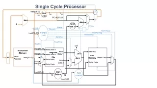
P C S r c 0 A d d M Clock u x R e g W r i t e A L U 1 4 A d d r e s u l t S h i f t Clock M e m W r i t e l e f t 2 R e a d rs I n s t r u c t i o n [ 2 5 – 2 1 ] r e g i s t e r 1 R e a d d a t a 1 R e a d R e a d P C r e g i s t e r 2 Z e r o I n s t r u c t i o n [ 2 0 – 1 6 ] a d d r e s s R e a d M e m t o R e g A L U S r c A L U rt R e a d W r i t e d a t a 2 1 A d d r e s s r e s u l t I n s t r u c t i o n r e g i s t e r d a t a 0 M A L U [ 3 1 – 0 ] 0 W r i t e u M R e g i s t e r s x d a t a M u D a t a 0 I n s t r u c t i o n u I n s t r u c t i o n [ 1 5 – 1 1 ] W r i t e x m e m o r y x m e m o r y d a t a rd 1 3 2 clock S i g n I n s t r u c t i o n [ 1 5 – 0 ] 1 e x t e n d MemRead=1 MemWrite=0 R e g D s t 4 1 6 offset M e m R e a d ALU control Datapath for R-type, LW, SW & BEQ Figure 5.15 with additions in red Presentation G
0 M u x A L U A d d 1 r e s u l t A d d S h i f t P C S r c l e f t 2 R e g D s t 4 B r a n c h M e m R e a d M e m t o R e g I n s t r u c t i o n [ 3 1 2 6 ] C o n t r o l A L U O p M e m W r i t e A L U S r c R e g W r i t e I n s t r u c t i o n [ 2 5 2 1 ] R e a d R e a d r e g i s t e r 1 P C R e a d a d d r e s s d a t a 1 I n s t r u c t i o n [ 2 0 1 6 ] R e a d Z e r o r e g i s t e r 2 I n s t r u c t i o n 0 R e g i s t e r s A L U R e a d A L U [ 3 1 – 0 ] 0 R e a d W r i t e A d d r e s s M d a t a 2 r e s u l t 1 d a t a I n s t r u c t i o n r e g i s t e r M u M u m e m o r y x u I n s t r u c t i o n [ 1 5 1 1 ] W r i t e x D a t a 1 x d a t a 1 m e m o r y 0 W r i t e d a t a 1 6 3 2 I n s t r u c t i o n [ 1 5 0 ] S i g n e x t e n d A L U c o n t r o l I n s t r u c t i o n [ 5 0 ] Control Unit and Datapath opcode Clock anded rs Clock anded rt Clock rd MemRead=1 MemWrite=0 offset funct Figure 5.17 with additions in red Presentation G
Memto- Reg Mem Mem Op-code RegDst ALUSrc Reg Write Read Write Branch ALUOp1 ALUp0 000000 1 0 0 1 d 0 0 1 0 100011 0 1 1 1 1 0 0 0 0 101011 d 1 d 0 0 1 0 0 0 000100 d 0 d 0 d 0 1 0 1 Input Output Truth Table for (Main) Control Unit • ALUOp[1-0] = 00 signal to ALU Control unit for ALU to perform add • function, i.e. set Ainvert = 0, Binvert=0 and Operation=10 • ALUOp[1-0] = 01 signal to ALU Control unit for ALU to perform subtract • function, i.e. set Ainvert = 0, Binvert=1 and Operation=10 • ALUOp[1-0] = 10 signal to ALU Control unit to look at bits I[5-0] and based • on its pattern to set Ainvert, Binvert and Operation so • that ALU performs appropriate function, i.e. add, sub, slt, • and, or & nor R-type lw sw beq Presentation G
Input Output ALUOp Funct field ALU Control ALUOp1 ALUOp0 F5 F4 F3 F2 F1 F0 add sub add sub and or slt nor 0 0 d d d d d d 0 0 10 0 1 d d d d d d 0 1 10 1 0 1 0 0 0 0 0 0 0 10 1 0 1 0 0 0 1 0 0 1 10 1 0 1 0 0 1 0 0 0 0 00 1 0 1 0 0 1 0 1 0 0 01 1 0 1 0 1 0 1 0 0 1 11 1 0 1 0 1 0 0 1 1 1 00 Truth Table of ALU Control Unit Ainvert BivertOperation
Op-code bits 5 4 3 2 1 0 Memto- Reg Mem Mem RegDst ALUSrc Reg Write Read Write Branch ALUOp1 ALUp0 0 0 0 0 0 0 1 0 0 1 d 0 0 1 0 I n p u t s 1 0 0 0 1 1 0 1 1 1 1 0 0 0 0 O p 5 1 0 1 0 1 1 d 1 d 0 0 1 0 0 0 O p 4 O p 3 0 0 0 1 0 0 d 0 d 0 d 0 1 0 1 O p 2 O p 1 O p 0 O u t p u t s R - f o r m a t I w s w b e q R e g D s t A L U S r c M e m t o R e g R e g W r i t e M e m R e a d M e m W r i t e B r a n c h A L U O p 1 A L U O p O Design of (Main) Control Unit 0 0 … 0 … 0 Figure C.2.5 RegDst =Op5Op4Op3Op2Op1Op0 ALUSrc= Op5Op4Op3Op2Op1Op0 +Op5Op4Op3Op2Op1Op0
31 26 25 0 j jump_target P C + 4 [ 3 1 – 2 8 ] J u m p a d d r e s s [ 3 1 – 0 ] I n s t r u c t i o n [ 2 5 – 0 ] S h i f t l e f t 2 2 6 2 8 0 1 M M u u x x A L U A d d 1 0 r e s u l t shift left 2 A d d R e g D s t J u m p 4 B r a n c h M e m R e a d I n s t r u c t i o n [ 3 1 – 2 6 ] M e m t o R e g C o n t r o l A L U O p M e m W r i t e A L U S r c R e g W r i t e I n s t r u c t i o n [ 2 5 – 2 1 ] R e a d R e a d r e g i s t e r 1 P C R e a d a d d r e s s d a t a 1 I n s t r u c t i o n [ 2 0 – 1 6 ] R e a d Z e r o r e g i s t e r 2 I n s t r u c t i o n 0 R e g i s t e r s A L U R e a d A L U [ 3 1 – 0 ] 0 R e a d W r i t e M d a t a 2 A d d r e s s r e s u l t 1 d a t a I n s t r u c t i o n r e g i s t e r M u M u m e m o r y x u I n s t r u c t i o n [ 1 5 – 1 1 ] W r i t e x 1 D a t a x d a t a 1 m e m o r y 0 W r i t e d a t a 1 6 3 2 I n s t r u c t i o n [ 1 5 – 0 ] S i g n e x t e n d A L U c o n t r o l I n s t r u c t i o n [ 5 – 0 ] Datapath for R-type, LW, SW, BEQ & J PC PC31-28 || jump_target || 00 Add 2 zeros PC[31-28] Figure 5.24 with correction in red
Op-code bits 5 4 3 2 1 0 Memto- Reg Mem Mem RegDst ALUSrc Reg Write Read Write Branch ALUOp1 ALUp0 0 0 0 0 0 0 1 0 0 1 d 0 0 1 0 1 0 0 0 1 1 0 1 1 1 1 0 0 0 0 1 0 1 0 1 1 d 1 d 0 0 1 0 0 0 0 0 0 1 0 0 d 0 d 0 d 0 1 0 1 I n p u t s O p 5 O p 4 O p 3 Jump =Op5Op4Op3Op2Op1Op0 O p 2 O p 1 O p 0 Jump R - f o r m a t I w s w b e q R e g D s t A L U S r c M e m t o R e g R e g W r i t e M e m R e a d M e m W r i t e B r a n c h A L U O p 1 A L U O p O Design of Control Unit (J included) Jump 0 0 0 0 1 J 0 0 0 0 1 0 d d d 0 d 0 d d d … 0 No changes in ALU Control unit
Input Output ALUOp Funct field ALU Control A L U O P 1 A L U O P 0 ALUOp1 ALUOp0 F5 F4 F3 F2 F1 F0 0 0 d d d d d d 010 0 1 d d d d d d 110 F 5 1 0 1 0 0 0 0 0 010 F 4 1 0 1 0 0 0 1 0 110 F 3 1 0 1 0 0 1 0 0 000 1 0 1 0 0 1 0 1 001 F 2 1 0 1 0 1 0 1 0 111 F 1 F 0 Design of 7-Function ALU Control Unit add sub add sub and or slt BivertOperation Figure C.2.3 with improvements ALU Control Lines (Binvert & Operation)
Cycle Time Calculation • Let us assume that the onlydelays introduced are by the following tasks: • Memory access (read and write time = 3 nsec) • Register file access (read and write time = 1 nsec) • ALU to perform function (= 2 nsec) • Under those assumption here are instruction execution times: Instr Reg ALU Data Reg fetch read oper memory write Total R-type 3 + 1 + 2 + 1 = 7 nsec lw 3 + 1 + 2 + 3 + 1 = 10 nsec sw 3 + 1 + 2 + 3 = 9 nsec branch 3 + 1 + 2 = 6 nsec jump 3 = 3 nsec • Thus a clock cycle time has to be 10nsec, and clock rate = 1/10 nsec = 100MHz Presentation G
Single Cycle Processor: Conclusion • Single Cycle Problems: • what if we had a more complicated instruction like floating point? • a clock cycle would be much longer, • thus for shorter and more often used instructions, such as add & lw, wasteful of time. • One Solution: • use a “smaller” cycle time, and • have different instructions take different numbers of cycles. • And that is a “multi-cycle” processor. Presentation G
Datapath for R-type, LW, SW, BEQ & J Add 2 zeros J u m p a d d r e s s [ 3 1 – 0 ] I n s t r u c t i o n [ 2 5 – 0 ] 2 6 2 8 PC[31-28] 0 1 M M u u x x A L U A d d 1 0 r e s u l t shift left 2 A d d R e g D s t J u m p 4 B r a n c h M e m R e a d I n s t r u c t i o n [ 3 1 – 2 6 ] M e m t o R e g C o n t r o l A L U O p M e m W r i t e A L U S r c R e g W r i t e I n s t r u c t i o n [ 2 5 – 2 1 ] R e a d R e a d r e g i s t e r 1 P C R e a d a d d r e s s d a t a 1 I n s t r u c t i o n [ 2 0 – 1 6 ] R e a d Z e r o r e g i s t e r 2 I n s t r u c t i o n 0 R e g i s t e r s A L U R e a d A L U [ 3 1 – 0 ] 0 R e a d W r i t e M d a t a 2 A d d r e s s r e s u l t 1 d a t a I n s t r u c t i o n r e g i s t e r M u M u m e m o r y x u I n s t r u c t i o n [ 1 5 – 1 1 ] W r i t e x 1 D a t a x d a t a 1 m e m o r y 0 W r i t e d a t a 1 6 3 2 I n s t r u c t i o n [ 1 5 – 0 ] S i g n e x t e n d A L U c o n t r o l I n s t r u c t i o n [ 5 – 0 ]
Control Unit Truth Table and Design Op-code bits 5 4 3 2 1 0 Memto- Reg Mem Mem RegDst ALUSrc Reg Write Read Write Branch ALUOp1 ALUp0 0 0 0 0 0 0 1 0 0 1 d 0 0 1 0 1 0 0 0 1 1 0 1 1 1 1 0 0 0 0 1 0 1 0 1 1 d 1 d 0 0 1 0 0 0 0 0 0 1 0 0 d 0 d 0 d 0 1 0 1 I n p u t s O p 5 O p 4 O p 3 O p 2 O p 1 O p 0 Jump R - f o r m a t I w s w b e q R e g D s t A L U S r c M e m t o R e g R e g W r i t e M e m R e a d M e m W r i t e B r a n c h A L U O p 1 A L U O p O Jump 0 0 0 0 1 0 0 0 0 1 0 d d d 0 d 0 d d d