Download
1 / 52
520 likes | 706 Views
Single Cycle Datapath. Lecture notes from MKP, H. H. Lee and S. Yalamanchili. Reading. Section 4.1-4.4 Appendices C.7, C.8, C.11, D.2 Practice Problems: 1, 4, 6, 9. Introduction. We will examine two MIPS implementations A simplified version this module

E N D
Single Cycle Datapath Lecture notes from MKP, H. H. Lee and S. Yalamanchili
Reading • Section 4.1-4.4 • Appendices C.7, C.8, C.11, D.2 • Practice Problems: 1, 4, 6, 9
Introduction • We will examine two MIPS implementations • A simplified version this module • A more realistic pipelined version • Simple subset, shows most aspects • Memory reference: lw, sw • Arithmetic/logical: add, sub, and, or, slt • Control transfer: beq, j
Instruction Execution • PC instruction memory, fetch instruction • Register numbers register file, read registers • Depending on instruction class • Use ALU to calculate • Arithmetic result • Memory address for load/store • Branch target address • Access data memory for load/store • PC An address or PC + 4 An Encoded Program 8d0b0000 014b5020 21080004 2129ffff 1520fffc 000a082a ….. ….. Address
Basic Ingredients • Include the functional units we need for each instruction – combinational and sequential A L U c o n t r o l 5 3 R e a d r e g i s t e r 1 R e a d d a t a 1 5 R e g i s t e r R e a d Z e r o r e g i s t e r 2 n u m b e r s R e g i s t e r s D a t a A L U A L U 5 W r i t e r e s u l t r e g i s t e r R e a d d a t a 2 W r i t e D a t a d a t a R e g W r i t e a . R e g i s t e r s b . A L U
D Q Clk Clk D Q Sequential Elements (4.2, C.7, C.11) • Register: stores data in a circuit • Uses a clock signal to determine when to update the stored value • Edge-triggered: update when Clk changes from 0 to 1 falling edge rising edge
Clk D Q Write Write D Clk Q Sequential Elements • Register with write control • Only updates on clock edge when write control input is 1 • Used when stored value is required later cycle time
Clocking Methodology • Combinational logic transforms data during clock cycles • Between clock edges • Input from state elements, output to state element • Longest delay determines clock period • Synchronous vs. Asynchronous operation Recall: Critical Path Delay
Register File (C.8) • Built using D flip-flops (remember ECE 2030!)
Register File • Note: we still use the real clock to determine when to write
Building a Datapath (4.3) • Datapath • Elements that process data and addressesin the CPU • Registers, ALUs, mux’s, memories, … • We will build a MIPS datapath incrementally • Refining the overview design
High Level Description Control • Single instruction single data stream model of execution (Remember Flynn’s Taxonomy) • Serial execution model • Commonly known as the von Neumann execution model • Stored program model • Instructions and data share memory Fetch Instructions Execute Instructions Memory Operations Data Streams SISD SIMD Instruction Streams MISD MIMD
Instruction Fetch Increment by 4 for next instruction clk 32-bit register cycle time Start instruction fetch Complete instruction fetch clk
R-Format Instructions • Read two register operands • Perform arithmetic/logical operation • Write register result op rs rt rd shamt funct
Executing R-Format Instructions 3 A L U c o n t r o l 5 R e a d r e g i s t e r 1 R e a d d a t a 1 5 R e a d Z e r o r e g i s t e r 2 A L U A L U 5 W r i t e r e s u l t r e g i s t e r R e a d d a t a 2 W r i t e d a t a R e g W r i t e op rs rt rd shamt funct
Load/Store Instructions • Read register operands • Calculate address using 16-bit offset • Use ALU, but sign-extend offset • Load: Read memory and update register • Store: Write register value to memory op rs rt 16-bit constant
R e a d r e g i s t e r 1 Executing I-Format Instructions M e m W r i t e R e a d r e g i s t e r 2 R e a d A d d r e s s W r i t e d a t a r e g i s t e r D a t a W r i t e m e m o r y d a t a R e g W r i t e 1 6 3 2 S i g n M e m R e a d e x t e n d op rs rt 16-bit constant
Branch Instructions • Read register operands • Compare operands • Use ALU, subtract and check Zero output • Calculate target address • Sign-extend displacement • Shift left 2 places (word displacement) • Add to PC + 4 • Already calculated by instruction fetch op rs rt 16-bit constant
Branch Instructions Justre-routes wires Sign-bit wire replicated op rs rt 16-bit constant
Updating the Program Counter Branch 0 M A d d u x Computation of the branch address A L U 1 4 A d d r e s u l t S h i f t I n s t r u c t i o n [ 2 5 – 2 1 ] R e a d P C I n s t r u c t i o n [ 2 0 – 1 6 ] a d d r e s s I n s t r u c t i o n [ 3 1 – 0 ] loop: beq $t0, $0, exit addi $t0, $t0, -1 lw $a0, arg1($t1) lw $a1, arg2($t2) jal func add $t3, $t3, $v0 addi $t1, $t1, 4 addi $t2, $t2, 4 j loop I n s t r u c t i o n I n s t r u c t i o n [ 1 5 – 1 1 m e m o r y 1 6 3 2 S i g n I n s t r u c t i o n [ 1 5 – 0 ] e x t e n d
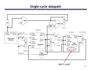
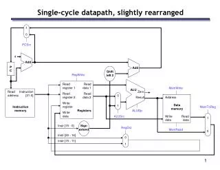
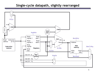
Composing the Elements • First-cut data path does an instruction in one clock cycle • Each datapath element can only do one function at a time • Hence, we need separate instruction and data memories • Use multiplexers where alternate data sources are used for different instructions An Encoded Program 014b5020 21080004 2129ffff 1520fffc 000a082a ….. ….. PC Address
Full Single Cycle Datapath Destination register is “instruction-specific”
0 4 35 or 43 rs rs rs rt rt rt rd address address shamt funct 31:26 31:26 31:26 25:21 25:21 25:21 20:16 20:16 20:16 15:11 10:6 15:0 15:0 5:0 The Main Control Unit • Control signals derived from instruction R-type Load/Store Branch opcode always read read, except for load write for R-type and load sign-extend and add
ALU Control (4.4, D.2) • ALU used for • Load/Store: Functon= add • Branch: Function = subtract • R-type: Function depends on funct field
ALU Control • Assume 2-bit ALUOp derived from opcode • Combinational logic derives ALU control • How do we turn this description into gates?
A L U c o n t r o l 3 ALUOp Funct field ALU Control ALUOp1 ALUOp0 F5 F4 F3 F2 F1 F0 Z e r o A L U A L U 0 0 X X X X X X 010 r e s u l t X 1 X X X X X X 110 1 X X X 0 0 0 0 010 1 X X X 0 0 1 0 110 1 X X X 0 1 0 0 000 1 X X X 0 1 0 1 001 1 X X X 1 0 1 0 111 ALU Controller ALUOp funct = inst[5:0] ALU control lw/sw add beq sub add sub arith and or slt Generated from Decoding inst[31:26] inst[5:0]
ALU Control • Simple combinational logic (truth tables)
Memto- Reg Mem Mem Instruction RegDst ALUSrc Reg Write Read Write Branch ALUOp1 ALUp0 R-format 1 0 0 1 0 0 0 1 0 lw 0 1 1 1 1 0 0 0 0 sw X 1 X 0 0 1 0 0 0 beq X 0 X 0 0 0 1 0 1 Datapath With Control (4.5) Use rt not rd
Commodity Processors ARM 7 Single Cycle Datapath
Memto- Reg Mem Mem Instruction RegDst ALUSrc Reg Write Read Write Branch ALUOp1 ALUp0 R-format 1 0 0 1 0 0 0 1 0 lw 0 1 1 1 1 0 0 0 0 sw X 1 X 0 0 1 0 0 0 beq X 0 X 0 0 0 1 0 1 Control Unit Signals Inst[31:26] To harness the datapath
Controller Implementation LIBRARY IEEE; USE IEEE.STD_LOGIC_1164.ALL; USE IEEE.STD_LOGIC_ARITH.ALL; USE IEEE.STD_LOGIC_SIGNED.ALL; ENTITY control IS PORT( SIGNAL Opcode : IN STD_LOGIC_VECTOR( 5 DOWNTO 0 ); SIGNAL RegDst : OUT STD_LOGIC; SIGNAL ALUSrc : OUT STD_LOGIC; SIGNAL MemtoReg : OUT STD_LOGIC; SIGNAL RegWrite : OUT STD_LOGIC; SIGNAL MemRead : OUT STD_LOGIC; SIGNAL MemWrite : OUT STD_LOGIC; SIGNAL Branch : OUT STD_LOGIC; SIGNAL ALUop: OUT STD_LOGIC_VECTOR( 1 DOWNTO 0 ); SIGNAL clock, reset : IN STD_LOGIC ); END control;
Memto- Reg Mem Mem Instruction RegDst ALUSrc Reg Write Read Write Branch ALUOp1 ALUp0 R-format 1 0 0 1 0 0 0 1 0 lw 0 1 1 1 1 0 0 0 0 sw X 1 X 0 0 1 0 0 0 beq X 0 X 0 0 0 1 0 1 Controller Implementation (cont.) ARCHITECTURE behavior OF control IS SIGNAL R_format, Lw, Sw, Beq : STD_LOGIC; BEGIN -- Code to generate control signals using opcode bits R_format <= '1' WHEN Opcode = "000000" ELSE '0'; Lw <= '1' WHEN Opcode = "100011" ELSE '0'; Sw <= '1' WHEN Opcode = "101011" ELSE '0'; Beq <= '1' WHEN Opcode = "000100" ELSE '0'; RegDst <= R_format; ALUSrc <= Lw OR Sw; MemtoReg <= Lw; RegWrite <= R_format OR Lw; MemRead <= Lw; MemWrite <= Sw; Branch <= Beq; ALUOp( 1 ) <= R_format; ALUOp( 0 ) <= Beq; END behavior; Implementation of each table column
2 address 31:26 25:0 Implementing Jumps • Jump uses word address • Update PC with concatenation of • Top 4 bits of old PC • 26-bit jump address • 00 • Need an extra control signal decoded from opcode Jump
Energy Behavior combinational activity storage read/write access
Vdd PMOS Vin Vout NMOS Ground Recall Hierarchy of Energy Models Aggregate energy into higher level modules ALU a Aggregate energy expenditure into gate level estimates x b c y Switch level activity (dynamic) and leakage (static) energy costs
A Simple Architecture Energy Model • To a first order, we can use the per-access energy of each major component • Obtain this for a technology generation • Use this per-access energy to compute the energy of each instruction • Note: • This is a high level approximation. The actual physics is more complicated. • However, this useful for several purposes • What components do each instruction exercise?
Example: Updating the PC Branch 0 M A d d u x A L U 1 4 A d d r e s u l t What is the energy cost of this operation? S h i f t R e g W r i t e l e f t 2 I n s t r u c t i o n [ 2 5 – 2 1 ] R e a d r e g i s t e r 1 R e a d M e m W r i t e R e a d P C d a t a 1 I n s t r u c t i o n [ 2 0 – 1 6 ] a d d r e s s R e a d M e m t o R e g A L U S r c r e g i s t e r 2 Z e r o I n s t r u c t i o n R e a d 0 A L U A L U [ 3 1 – 0 ] 0 R e a d W r i t e d a t a 2 1 A d d r e s s r e s u l t M r e g i s t e r M d a t a u M I n s t r u c t i o n u I n s t r u c t i o n [ 1 5 – 1 1 ] x W r i t e u x m e m o r y R e g i s t e r s x 1 d a t a 1 D a t a 0 W r i t e m e m o r y R e g D s t d a t a 1 6 3 2 S i g n I n s t r u c t i o n [ 1 5 – 0 ] e x t e n d A L U M e m R e a d c o n t r o l I n s t r u c t i o n [ 5 – 0 ] A L U O p
Example: Register Instructions Branch 0 M A d d u x A L U 1 4 A d d r e s u l t What is the energy cost of this operation? S h i f t R e g W r i t e l e f t 2 I n s t r u c t i o n [ 2 5 – 2 1 ] R e a d r e g i s t e r 1 R e a d M e m W r i t e R e a d P C d a t a 1 I n s t r u c t i o n [ 2 0 – 1 6 ] a d d r e s s R e a d M e m t o R e g A L U S r c r e g i s t e r 2 Z e r o I n s t r u c t i o n R e a d 0 A L U A L U [ 3 1 – 0 ] 0 R e a d W r i t e d a t a 2 1 A d d r e s s r e s u l t M r e g i s t e r M d a t a u M I n s t r u c t i o n u I n s t r u c t i o n [ 1 5 – 1 1 ] x W r i t e u x m e m o r y R e g i s t e r s x 1 d a t a 1 D a t a 0 W r i t e m e m o r y R e g D s t d a t a 1 6 3 2 S i g n I n s t r u c t i o n [ 1 5 – 0 ] e x t e n d A L U M e m R e a d c o n t r o l I n s t r u c t i o n [ 5 – 0 ] A L U O p
Example: I-type Instructions Branch 0 M A d d u x A L U 1 4 A d d r e s u l t What is the energy cost of this operation? S h i f t R e g W r i t e l e f t 2 I n s t r u c t i o n [ 2 5 – 2 1 ] R e a d r e g i s t e r 1 R e a d M e m W r i t e R e a d P C d a t a 1 I n s t r u c t i o n [ 2 0 – 1 6 ] a d d r e s s R e a d M e m t o R e g A L U S r c r e g i s t e r 2 Z e r o I n s t r u c t i o n R e a d 0 A L U A L U [ 3 1 – 0 ] 0 R e a d W r i t e d a t a 2 1 A d d r e s s r e s u l t M r e g i s t e r M d a t a u M I n s t r u c t i o n u I n s t r u c t i o n [ 1 5 – 1 1 ] x W r i t e u x m e m o r y R e g i s t e r s x 1 d a t a 1 D a t a 0 W r i t e m e m o r y R e g D s t d a t a 1 6 3 2 S i g n I n s t r u c t i o n [ 1 5 – 0 ] e x t e n d A L U M e m R e a d c o n t r o l I n s t r u c t i o n [ 5 – 0 ] A L U O p
0 M A d d u x A L U 1 4 A d d r e s u l t S h i f t R e g W r i t e l e f t 2 Branch I n s t r u c t i o n [ 2 5 – 2 1 ] R e a d r e g i s t e r 1 R e a d M e m W r i t e R e a d P C d a t a 1 I n s t r u c t i o n [ 2 0 – 1 6 ] a d d r e s s R e a d M e m t o R e g A L U S r c r e g i s t e r 2 Z e r o I n s t r u c t i o n R e a d 0 A L U A L U [ 3 1 – 0 ] 0 R e a d W r i t e d a t a 2 1 A d d r e s s r e s u l t M r e g i s t e r M d a t a u M I n s t r u c t i o n u I n s t r u c t i o n [ 1 5 – 1 1 ] x W r i t e u x m e m o r y R e g i s t e r s x 1 d a t a 1 D a t a 0 W r i t e m e m o r y R e g D s t d a t a 1 6 3 2 S i g n I n s t r u c t i o n [ 1 5 – 0 ] e x t e n d A L U M e m R e a d c o n t r o l I n s t r u c t i o n [ 5 – 0 ] A L U O p Example: I-Type for Branches What is the energy cost of this operation?
Converting Energy to Power • For this data path, except for data memory, all components are active every cycle, and dissipating energy on every cycle • Later we will see how data paths can be made more energy efficient • Computing power • Compute the total energy consumed over all cycles (instructions) • Divide energy by time to get power in watts Example:
ITRS Roadmap for Logic Devices From: “ExaScaleComputing Study: Technology Challenges in Achieving Exascale Systems,” P. Kogge, et.al, 2008
Our Simple Control Structure • All of the logic is combinational • We wait for everything to settle down, and the right thing to be done • ALU might not produce “right answer” right away • we use write signals along with clock to determine when to write • Cycle time determined by length of the longest path We are ignoring some details like setup and holdtimes
Performance Issues • Longest delay determines clock period • Critical path: load instruction • Instruction memory register file ALU data memory register file • Not feasible to vary period for different instructions • Violates design principle • Making the common case fast • We will improve performance by pipelining
Summary • Single cycle datapath • All instructions execute in one clock cycle • Not all instructions take the same amount of time • Software sees a simple interface • Can memory operations really take one cycle? • Improve performance via pipelining, multi-cycle operation, parallelism or customization • We will address these next
Study Guide • Given an instruction, be able to specify the values of all control signals required to execute that instruction • Add new instructions: modify the datapath and control to affect its execution • E.g., jal, jr, shift, etc. • Modify the VHDL controller • Given delays of various components, determine the cycle time of the datapath • Distinguish between those parts of the datapath that are unique to each instruction and those components that are shared across all instructions