Download
1 / 22
240 likes | 492 Views
Viterbi Decoder Project. Alon weinberg, Dan Elran Supervisors: Emilia Burlak, Elisha Ulmer. General.

E N D
Viterbi Decoder Project Alon weinberg, Dan Elran Supervisors: Emilia Burlak, Elisha Ulmer
General In this project we will implement the Viterbi Digital channel decoding algorithm both in hardware and in software on a Qualcomm Israel based platform, in order to learn about digital communication channels, the algorithm itself, the board and the working interface (SW/HW)
Project Goals • Studying the Viterbi algorithm and the convolutional code • Viterbi decoder implementation • Studying the board on which the implementation will take place • Studying the TI DSP on board • Studying the arbiter and busses (synch. And async.) on board • PCI bus and interface (study and implementation) • H\W – Software interface (DSP – FPGAs) • H\W-software work load • RAM model configuration • RAM interface module implementation • Working in high frequencies (theory+implementation) • Good VHDL and C DSP programming knowledge and abilities
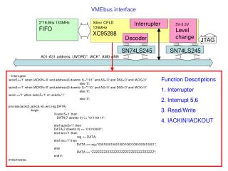
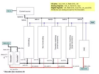
Board usage We will implement on the DSP the software part which will contain the Chainback initiation module and interface to the hardware. On the FPGA we will implement the hardware part, which includes the ACS and branch metric blocks as well as interface from the FPGA to the DSP. There will be a Dual Port Ram on the FPGA in order to pass data between HW and SW. In general the software will control the HW By control registers.
Board bus rates • DSP works at 160 MHz • BUT Arbiter works at 40 MHz (Bottleneck) • Periferial BUS (PCI) • Local Bus • PLX and DSP can master both buses • Asynched I/O FIFOs connected to FPGAs
Viterbi Decoding Algorithm • The Viterbi decoding algorithm is a state of the art algorithm used to decode convolutional binary codes (viewd as a trellis tree) used in communication standards (like Qualcomm’s CDMA standard). • The Viterbi decoder operates by finding the most likely decoding sequence for an input code symbol stream.
Convolutional codes Convolutional codes add correlation to the input data sequence by using delay elements and modulo adders. Binary convolutional encoders can be implemented with a feed forward shift register and exclusive or (XOR) gates.
Convolutional codes (cont.) Input bits enter the shift register one bit at a time. The outputs of the generator functions become the encoded output symbols. Each of the generator functions produce an output symbol for each input bit. The number of delay elements in the SHR define the state of the encoder and the constraint length. An encoder containing N memory elements has 2^N possible states and a K=N+1 constraint length.
Viterbi Decoding The Viterbi decoder finds the most likely path through the encoder Trellis. The 3 main steps in the process are : • Branch metric generation • State metric generation • Chainback
Implementation considerations • Fully parallel- N Trellis states are processed in parallel and each cycle a whole Trellis column is ready. This way we can also calculate the most likely state during the process and only output the decision bit. Easy for H/W implementation, fast. Takes a lot of FPGA space and resources (exponential with K). Not commonly used.
Implementation considerations (cont.) • Fully serial- each cycle one state is ready. N cycles to process one whole Trellis column. More difficult H/W implementation, N times slower. Takes a little FPGA space without any correlation to K (fixed amount of space taken). • Partially parallel-serial- m<N states processed each cycle. Choose m by space and speed considerations (bigger m: faster, more space).
Implementation considerations (cont.) Since the chip is used in a mobile cellular phone, it should be very small, but still fast enough in order to prevent delays in the data stream (the conversation). We chose the fully serial implementation, due to H/W bottleneck (board bus and SW working rates). Today most of the implementations are partially serial-parallel, with a small m (2- 4).
Software implementation The software will have two major roles: • The Chainback block Receives the state metrics calculated in H/W and chains back the Trellis to find the most likely path. • General control of the whole process (control the H/W through the control registers).
Software implementation (cont.) The software will run on the DSP, over the VX Works operating systems (which is the real time operating systems used on the CPU card). The code for the DSP will be written in the C language.